
List of Semiconductor Manufacturing Equipment products
- classification:Semiconductor Manufacturing Equipment
1~45 item / All 5250 items


It won't break even after 1 million repetitions! A mat switch with reliable operation, high durability, and low price. Suitable for options in machine tools as well. Please consult us about delivery t...
- Sensors


We can accommodate high resistance over 10,000 ohms, with diameters ranging from approximately 30 mm to 8 inches, and we also offer thinning and chip processing arrangements!
- Other semiconductors
- Processing Contract
- Wafer


Maximum operating temperature 2000℃ Semi-automatic control Ultra-high temperature experimental furnace (carbon furnace, tungsten metal furnace) Compact and space-saving experimental furnace
- Heating device
- Annealing furnace
- Electric furnace

VOXIA compact X-ray CT imaging device
Compact design with a space-saving layout that can be installed anywhere. Despite its compact body, it generates high-resolution data through advanced calculation software. * X-ray tube voltage: 20-90kV, or 40-maximum 130kV * Focus diameter: 7μm (5μm@4W) * Detector pixel: 89μm, approximately 3.2 million pixels! * Sample size: Φ120mm ◉ Vcap (Control Software): A custom-made imaging stage tailored to the subject and purpose. A series of tasks from shooting to image output can be performed with just a click. High-speed continuous shooting in as fast as 20 seconds, with processing from shooting start to image reconstruction taking about 30 seconds. ◉ VCT (Reconstruction Software): Customizable automatic measurement and analysis software specialized for the specified subject. High-speed reconstruction of shooting data with 992 x 992 pixel images and 600 projections in just 3.8 seconds! ◉ MolcerPlus (3D Display Analysis): Custom software that enables measurement conditions that were difficult with conventional software. Software for displaying, processing, and measuring the imaged object. ● High safety, ● Compatible with a wide variety of samples, ● Intuitive HMI, easy operation.

Maximum operating temperature 2000℃ Semi-automatic control Ultra-high temperature experimental furnace (carbon furnace, tungsten metal furnace) Compact and space-saving experimental furnace
- Heating device
- Annealing furnace
- Electric furnace

4-Yen Multi-Sputtering Device 【MiniLab-S060】
4 cathodes with Φ2 inch configuration Simultaneous film deposition: 3-component simultaneous deposition (RF 500W or DC 850W) + HiPIMS (PulseDC 5KW) x 1 Power distribution and configuration settings for 4 cathodes can be freely changed via the HMI screen using the plasma relay switch 3 MFC systems (Ar, O2, N2) for reactive sputtering RIE etching stage RF 300W (main chamber) + <30W soft etching (LL chamber) Substrate heating: Max 500℃, 800℃, or 1000℃ (C/C or SiC coating) Substrate rotation and vertical movement (automatically controlled by stepping motor) APC automatic control: Upstream (MFC flow adjustment) or downstream (automatic valve opening adjustment on the exhaust side) Dimensions: 1,120(W) x 800(D) ● Mixed specifications for resistance heating deposition, organic material deposition, EB deposition, PECVD, etc. are also possible.

6 to 8 inch ultra-high temperature wafer annealing equipment, a high-performance machine that widely accommodates various purposes from research and development to small-scale production.
- Annealing furnace
VOXIA compact X-ray CT imaging device
Compact design with a space-saving layout that can be installed anywhere. Despite its compact body, it generates high-resolution data through advanced calculation software. * X-ray tube voltage: 20-90kV, or 40-maximum 130kV * Focus diameter: 7μm (5μm@4W) * Detector pixel: 89μm, approximately 3.2 million pixels! * Sample size: Φ120mm ◉ Vcap (Control Software): A custom-made imaging stage tailored to the subject and purpose. A series of tasks from shooting to image output can be performed with just a click. High-speed continuous shooting in as fast as 20 seconds, with processing from shooting start to image reconstruction taking about 30 seconds. ◉ VCT (Reconstruction Software): Customizable automatic measurement and analysis software specialized for the specified subject. High-speed reconstruction of shooting data with 992 x 992 pixel images and 600 projections in just 3.8 seconds! ◉ MolcerPlus (3D Display Analysis): Custom software that enables measurement conditions that were difficult with conventional software. Software for displaying, processing, and measuring the imaged object. ● High safety, ● Compatible with a wide variety of samples, ● Intuitive HMI, easy operation.

6 to 8 inch ultra-high temperature wafer annealing equipment, a high-performance machine that widely supports various purposes from research and development to small-scale production.
- Annealing furnace
- Heating device
- Electric furnace
4-Yen Multi-Sputtering Device 【MiniLab-S060】
4 cathodes with Φ2 inch configuration Simultaneous film deposition: 3-component simultaneous deposition (RF 500W or DC 850W) + HiPIMS (PulseDC 5KW) x 1 Power distribution and configuration settings for 4 cathodes can be freely changed via the HMI screen using the plasma relay switch 3 MFC systems (Ar, O2, N2) for reactive sputtering RIE etching stage RF 300W (main chamber) + <30W soft etching (LL chamber) Substrate heating: Max 500℃, 800℃, or 1000℃ (C/C or SiC coating) Substrate rotation and vertical movement (automatically controlled by stepping motor) APC automatic control: Upstream (MFC flow adjustment) or downstream (automatic valve opening adjustment on the exhaust side) Dimensions: 1,120(W) x 800(D) ● Mixed specifications for resistance heating deposition, organic material deposition, EB deposition, PECVD, etc. are also possible.
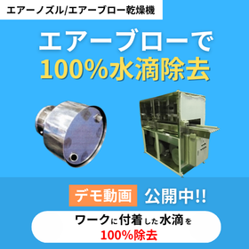

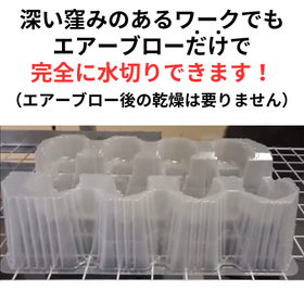
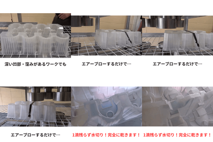
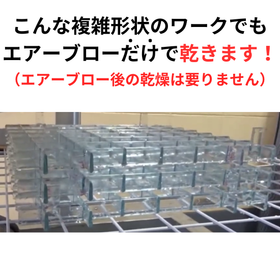
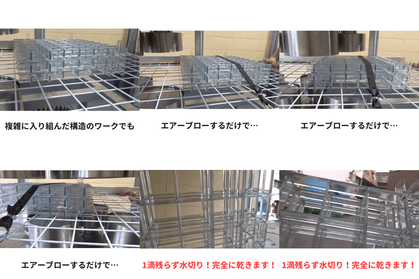
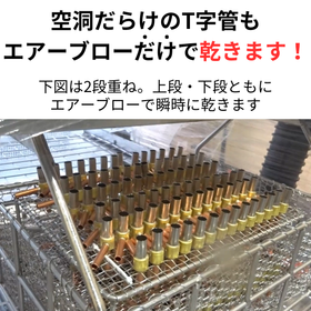
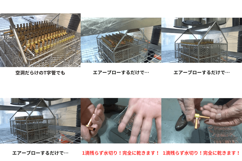
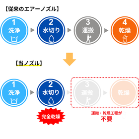
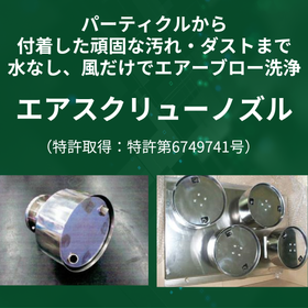
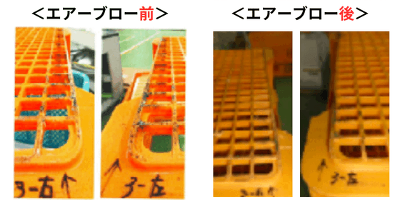
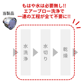
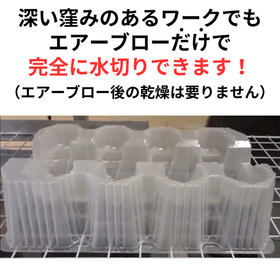
[Patent Obtained] Instant complete water removal of workpieces with air blow = complete drying!

- Other semiconductor manufacturing equipment

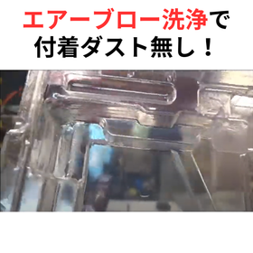
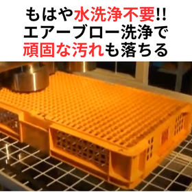
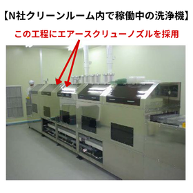
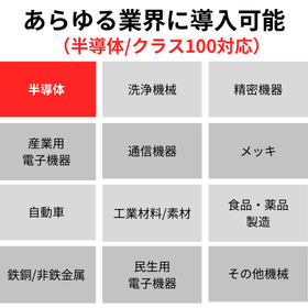
Revolutionary! No need for water washing! Particles are removed with just air blow.

- Other semiconductor manufacturing equipment
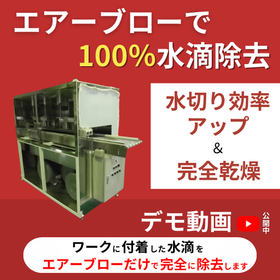
Are you making this mistake when draining water from your work?
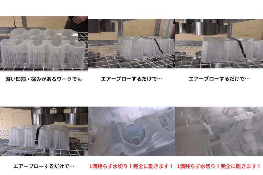
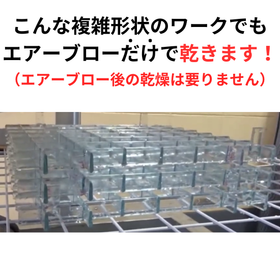
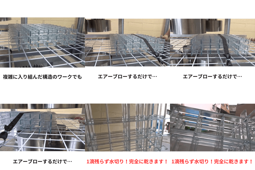
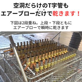
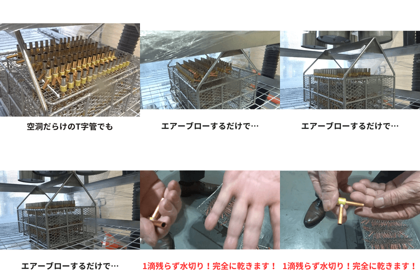
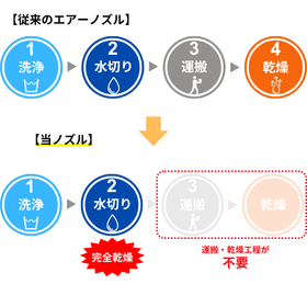

- Other semiconductor manufacturing equipment


Are you making this mistake with the work's drainage?


- Other semiconductor manufacturing equipment

Are you making this mistake while draining water from the work?
[To those in charge who are struggling with workpiece water drainage] Are you making these mistakes with workpiece water drainage? ✓ Do you know the real reason why, even if you increase the air blow pressure, not all water droplets are blown away? ✓ Do you know the real reason why, even if you increase the number of air nozzles, water is not sufficiently drained? ✓ Do you know the real reason why, even if you change the shape of the air nozzle, it still does not drain water effectively? These mistakes are typical errors made by companies that use air blow for workpiece water drainage and droplet removal. However, these mistakes are not significant compared to a certain "fatal mistake." What is that "fatal mistake"? It is… We provide this information in a PDF file. Download it now to find out.

No more revolution! No need for washing; particles are removed with just air blowing.


- Other semiconductor manufacturing equipment

Just by looking at this, you'll understand everything! We created a PR flyer (dust removal version).
Thoroughly remove dust from workpieces with air blow! We have summarized everything about the patented complete dust removal air nozzle, "Air Screw Nozzle," on a single A4 flyer. "What kind of nozzle is it?" "Why can it remove dust so effectively?" "How can it remove dust even from complex-shaped workpieces?" Just by looking at this, you can quickly understand everything about the Air Screw Nozzle. Please download and take a look.

[Patent Obtained] Complete water removal in an instant with air blow = complete drying!


- Other semiconductor manufacturing equipment

If you see this, you'll understand everything! I created a PR flyer.
100% water removal with air blow! No water droplets left on the workpiece! We have summarized everything about the patented complete drying air nozzle, "Air Screw Nozzle," on a single A4 flyer. "What kind of nozzle is it?" "Can it really remove 100% of the water?" "Why is it so effective at removing water?" Just by looking at this, you can quickly understand everything about the Air Screw Nozzle. Please download it and take a look!

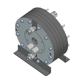
Ion exchange membrane electrolytic cell that achieves both high-purity oxidant production and gas separation.
- Other recycling systems
- Other surface treatment equipment
- Etching Equipment
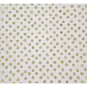

Easy diamond applications. You can trust us with peace of mind.
- Other semiconductors
- Wafer processing/polishing equipment


Meticulous work unique to Japanese manufacturers! Detailed follow-up visits by sales representatives even after installation.

- Wafer processing/polishing equipment
![[Column] Episode 1 Part 1 - Everyth...](https://image.mono.ipros.com/public/product/image/754/2000844313/IPROS87243123240253513930.jpeg?w=280&h=280)
I'm graduating from hand polishing!
- Wafer processing/polishing equipment
![[Column] Episode 1 Part 2 - Everyth...](https://image.mono.ipros.com/public/product/image/2e2/2000844332/IPROS13307731317786019679.jpeg?w=280&h=280)
I'm graduating from hand polishing!
- Wafer processing/polishing equipment
![[Column] Episode 2 Part 1 - Solve t...](https://image.mono.ipros.com/public/product/image/a5e/2000894172/IPROS07313810911026506019.jpeg?w=280&h=280)
~Me, Polishing, and IMT~
- Wafer processing/polishing equipment
![[Column] Episode 2 Part 2 - Solve t...](https://image.mono.ipros.com/public/product/image/43c/2000894173/IPROS92238813014816664627.jpeg?w=280&h=280)
~Me, Kenma, and IMT~
- Wafer processing/polishing equipment
![[Introduction] Sample Lab Center](https://image.mono.ipros.com/public/product/image/3bb/2000721861/IPROS98872278153279056483.png?w=280&h=280)
We will make proposals centered around polishing machines, polishing devices, and sample polishing machines, utilizing the know-how of all precision polishing technologies.


- Wafer processing/polishing equipment

Production of holders that meet your requests! We can create holders that respond to customer needs based on in-house design, and we are also capable of producing special shapes such as porous types a...


- Wafer processing/polishing equipment

Contributing to the simplification of inspection tasks with air-free semi-automatic polishing.


- Wafer processing/polishing equipment
![[Column] Episode 3 Part 1 - Manual ...](https://image.mono.ipros.com/public/product/image/51a/2000939251/IPROS69540763987577600618.jpeg?w=280&h=280)
~Me, Kenma, and IMT~
- Wafer processing/polishing equipment
![[Column] Episode 3 Part 2 - Manual ...](https://image.mono.ipros.com/public/product/image/159/2000939252/IPROS28817244719473077497.jpeg?w=280&h=280)
~Me, Kenma, and IMT~
- Wafer processing/polishing equipment

Perfect for creating high-precision samples! We are currently giving away a technical book that reveals the best polishing conditions, leading to process reduction and improved accuracy!!


- Wafer processing/polishing equipment

Ideal for high-precision sample preparation! We also propose optimal polishing conditions! Reliable domestic machines with comprehensive after-sales support!


- Wafer processing/polishing equipment

We respond to our customers' needs with a consistent production system that encompasses everything from design to assembly, with meticulous attention and a sense of speed.


- Wafer processing/polishing equipment
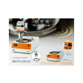
Presentation of Materials: Comprehensive Catalog of Grinding Machines for Integrated Production from Design to Assembly / IMT Corporation
IMT Corporation is a precision grinding equipment manufacturer headquartered in Wakayama. We previously had sales offices in Tokyo, Osaka, and Nagoya, but we have now decided to finally expand into Kyushu. Our company has been providing production equipment for the semiconductor and liquid crystal panel industries, as well as equipment for preparing materials for microscopic observation, for many years. Through our "domestic sample grinding machines" and "consumables for microscope sample preparation and grinding materials," we will consult on our customers' quality assurance operations. 【Features】 - Consistent support: A comprehensive production system from design to assembly in-house - Speedy response: Detailed and prompt service *For more details, please download the materials or contact us directly.

This is a new silicon wafer edge polishing device developed with the concept of space-saving and high throughput.
- Wafer processing/polishing equipment

High-Spec Dedicated Load Grinding Device


- Wafer processing/polishing equipment

A final polishing compound that enables the achievement of the highest level of polished surface when used in conjunction with the polishing cloth "Silica Final"!
- Wafer processing/polishing equipment
- Other abrasives

Particle size 0.045μm! A polishing agent that is difficult to agglomerate and settle, and can be dispersed in various organic solvents such as alcohol!
- Wafer processing/polishing equipment
- Other abrasives

Both overall and individual load polishing is possible! We offer a variety of interchangeable polishing discs tailored to your needs.

- Wafer processing/polishing equipment
- Other abrasives

Realization of low Ra using high-quality grinding tape.
- Wafer processing/polishing equipment

[Made in Japan] Precision Grinding Tape Used
- Wafer processing/polishing equipment

A semi-custom-made thin film experimental device that can be assembled with the desired configuration for processes such as sputtering, EB (electron beam), and annealing.
- Evaporation Equipment
- Sputtering Equipment
- Annealing furnace

The catalog for the MiniLab Flexible Thin Film Experimental Device has been renewed!
We have completely renewed the catalog for the MiniLab series thin film experimental equipment. 【Features of the MiniLab Series】 ◉ Supports sputtering, evaporation (resistive heating, organic, EB), annealing, plasma etching, etc. ◉ Modular design allows for flexible combinations of components (source hybrid types and multi-chamber configurations are possible) ◉ Compact, space-saving design (width 1,200 x depth 560 mm) ◉ Excellent operability: intuitive interface allows for centralized management of all operations via a touch panel without dispersion. We are confident that this will be of great assistance in research and development settings. Please consider it.

Two thin film experimental devices are connected with a load lock mechanism. Different film deposition devices (sputtering, evaporation, etc.) are seamlessly connected with the load lock.
- Sputtering Equipment
- Evaporation Equipment
- Etching Equipment

MiniLab-WCF Ultra High Temperature Wafer Annealing Furnace Max 2000℃_Dedicated for High-Temperature Wafer Sintering (6inch to 8inch)
Max 2000℃ Φ6〜8 inch wafer dedicated high-temperature annealing device, capable of small-scale production multi-atmosphere wafer annealing device. ◾️ Max 2000℃ ◾️ Effective heating range: Φ6〜Φ8 inch single wafer type or batch type (multi-stage 5 wafer cassette) ◾️ Heater control: 1 zone or 2 zones (cascade control) ◾️ Heater materials: ・C/C composite: Φ6〜Φ8 inch ・PG coating high-purity graphite: Φ6〜Φ8 inch ◾️ Operating atmosphere: ・Vacuum (1x10⁻²Pa), inert gas (Ar, N2) ◾️ PLC semi-automatic operation ・Automatic sequence control for vacuum/purge cycle and venting ・Fully automatic operation (optional) ・Touch panel operation, allowing centralized management without dispersed operations. ◾️ Process pressure control ・APC control (MFC flow or automatic opening adjustment valve PID loop control) ・Maximum 3 systems of MFC flow automatic control, or manual adjustment of float meter/needle valve ◾️ PLOT screen graph display, CSV data output

High-performance multi-sputtering device 6-element multi-sputter (for Φ4 inch) 4-element multi-sputter (for Φ6, 8 inch)
- Sputtering Equipment
- Evaporation Equipment
- Etching Equipment

◉Mini-BENCH-prism Semi-Automatic Ultra-High Temperature Experimental Furnace Max 2000℃
◉ Maximum operating temperature Max 2000℃ ◉ PLC semi-automatic control A higher model of the tabletop Mini-BENCH with semi-automatic control Automatically controls each process of "vacuum/purge cycle," "gas replacement," and "venting" Maximum operating temperature 2000℃ Semi-automatic control ultra-high temperature experimental furnace (carbon furnace, tungsten metal furnace) Compact and space-saving experimental furnace ◉ Effective heating range (crucible dimensions) - Planar heater heating range: Φ2 inch to Φ6 inch - Cylindrical heater heating range: Φ30 to Φ80 x Depth Max 100(H) mm ◉ Up to 3 MFC systems for automatic flow control (or manual adjustment) ◉ APC automatic pressure control ◉ Ensures safety during operation Monitors abnormal cooling water, chamber temperature, and overpressure. Made of SUS, the robust water-cooled chamber can be safely used even during continuous operation at maximum temperature. ◉ Compact and space-saving Width 603 x Depth 603 x Height 1,160 mm (*Installed inside rotary pump housing) Various sample heating experiments, such as ultra-high temperature heating of small samples and new material research and development, can be easily performed with simple operations. The main unit is compact yet can be used for research and development in various fields.

Max 1000℃, maximum 3 systems for MFC, APC pressure control, compatible with 4" or 6" substrates, high vacuum annealing equipment (<5 × 10^-7 mbar)
- Annealing furnace
◉Mini-BENCH-prism Semi-Automatic Ultra-High Temperature Experimental Furnace Max 2000℃
◉ Maximum operating temperature Max 2000℃ ◉ PLC semi-automatic control A higher model of the tabletop Mini-BENCH with semi-automatic control Automatically controls each process of "vacuum/purge cycle," "gas replacement," and "venting" Maximum operating temperature 2000℃ Semi-automatic control ultra-high temperature experimental furnace (carbon furnace, tungsten metal furnace) Compact and space-saving experimental furnace ◉ Effective heating range (crucible dimensions) - Planar heater heating range: Φ2 inch to Φ6 inch - Cylindrical heater heating range: Φ30 to Φ80 x Depth Max 100(H) mm ◉ Up to 3 MFC systems for automatic flow control (or manual adjustment) ◉ APC automatic pressure control ◉ Ensures safety during operation Monitors abnormal cooling water, chamber temperature, and overpressure. Made of SUS, the robust water-cooled chamber can be safely used even during continuous operation at maximum temperature. ◉ Compact and space-saving Width 603 x Depth 603 x Height 1,160 mm (*Installed inside rotary pump housing) Various sample heating experiments, such as ultra-high temperature heating of small samples and new material research and development, can be easily performed with simple operations. The main unit is compact yet can be used for research and development in various fields.

High-performance, cost-effective RF/DC magnetron sputtering device for research and development.
- Other semiconductor manufacturing equipment
- Sputtering Equipment
4-Yen Multi-Sputtering Device 【MiniLab-S060】
4 cathodes with Φ2 inch configuration Simultaneous film deposition: 3-component simultaneous deposition (RF 500W or DC 850W) + HiPIMS (PulseDC 5KW) x 1 Power distribution and configuration settings for 4 cathodes can be freely changed via the HMI screen using the plasma relay switch 3 MFC systems (Ar, O2, N2) for reactive sputtering RIE etching stage RF 300W (main chamber) + <30W soft etching (LL chamber) Substrate heating: Max 500℃, 800℃, or 1000℃ (C/C or SiC coating) Substrate rotation and vertical movement (automatically controlled by stepping motor) APC automatic control: Upstream (MFC flow adjustment) or downstream (automatic valve opening adjustment on the exhaust side) Dimensions: 1,120(W) x 800(D) ● Mixed specifications for resistance heating deposition, organic material deposition, EB deposition, PECVD, etc. are also possible.
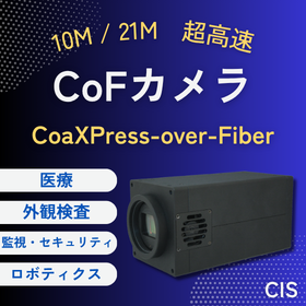

Supports high-speed semiconductor inspection and long-distance wiring. High resolution and high frame rate.
- Semiconductor inspection/test equipment
![[Printing Industry] Ultra High-Spee...](https://image.mono.ipros.com/public/product/image/2034982/IPROS11709385356860154695.png?w=280&h=280)
Accelerate the quality check of printed materials. Supports high resolution and long-distance transmission.
- Semiconductor inspection/test equipment


It excels in high sensitivity detection, quantification, and portability, making it suitable for quality inspection and research and development settings. It contributes to the detection of minute for...
- Semiconductor inspection/test equipment
- Other Sanitation Inspections
- Other appearance and image inspection equipment
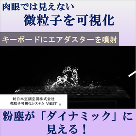
17th High-Performance Materials WEEK [Tokyo] We will be exhibiting a fine particle visualization system at the 17th High-Performance Film Exhibition. (September 30, 2026 (Wed) - October 2, 2026 (Fri) / Makuhari Messe, Hall 2)
The particle visualization technology developed under our brand "ViEST" has a very high level of detection sensitivity that allows for real-time visualization of the suspended and adhered states of micro and nano-sized particles. We are expanding our sales of visualization systems and providing evaluation services (such as investigating particles and airflow in production processes, manufacturing equipment, and factory environments, evaluating the performance of cleaning products, and proposing yield improvement measures) both domestically and internationally. We consistently support the identification of causes and the formulation of countermeasures by visualizing fine foreign substances, particle adhesion due to static electricity, and variations in cleanliness that are problematic in the film manufacturing process. The following are some examples of applications, but by utilizing our technology, we can strongly promote the resolution of various issues such as the deterioration of defect rates caused by fine foreign substances, visualization of clean airflow, and concerns regarding site cleanliness. - Visualization of foreign matter contamination and adhesion mechanisms in the coating and drying processes - Visualization of dust generation and re-adhesion during roll transportation and consideration of countermeasures - Evaluation of airflow and cleanliness within clean booths/clean rooms - Identification of dust sources within manufacturing equipment and promotion of cleanliness - Reduction of foreign matter adhesion risk on film surfaces and improvement of yield

Joining different materials without melting: A joining technology that balances precision and strength.
- Welding Machine
- Oxidation/Diffusion Device
- Processing Contract
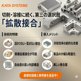
Please use it for demonstration tests and research and development.
- Processing Contract
- Contract manufacturing
- Semiconductor inspection/test equipment
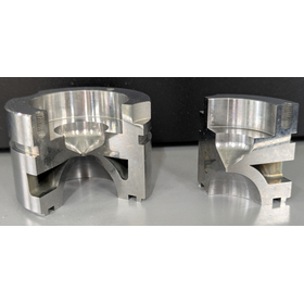
We meet the high precision needs of semiconductor manufacturing with microfabrication and diffusion bonding.
- Special Processing Machinery
- Heat exchanger
- Oxidation/Diffusion Device