We have a proven track record with a variety of chemical solutions! The reason for our low prices is that we handle everything in-house, from design to sales.
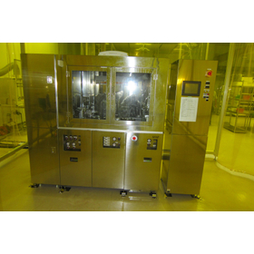
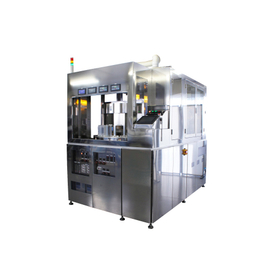
The development is performed by pooling the developer solution on the wafer in a batch process. Unlike the dip method, each wafer is developed individually, resulting in very high reproducibility of the process. By optimizing the amount of chemical used, it leads to a reduction in the amount of developer solution used. We can accommodate requests for pooling methods, from shower types to straight nozzles. It also features a shaking function during static development! (It moves the liquid by repeating low rotation and stopping.) The batch process includes development, rinsing, baking, and cooling functions. We design, manufacture, and sell according to customer needs and production volumes. We have a proven track record with various chemicals, including TMAH. 【Features】 ■ High reproducibility of development results ■ Reduction in chemical usage ■ Automatic wafer size recognition ■ Proven track record with various chemicals ■ Reduced footprint ■ Design tailored to production volume We have a permanent demo setup, so please consider a demonstration!

Inquire About This Product
basic information
【Main Specifications】 ■ Cassette Stage: 2 sets ■ Spin Development Unit: 2 sets ■ Wafer Size: Φ2" to Φ12" ■ Development Nozzle: 1 set/CUP ■ Rinse Nozzle: 1 set/CUP ■ Bake Unit: 4 sets (Max 200℃) ■ Cooling Unit: 2 sets ■ Centering Unit: 1 set ■ Equipment Size: (Example) 1400×1100×1800 (Φ4" main body) 400×900×1800 (Chemical supply + Power BOX) ■ Wafer Transport Robot: 1 set (Double Arm Clean Robot) Many other options available! *For more details, please feel free to contact us.
Price range
Delivery Time
※4 to 5 months (usually), but it may vary depending on the situation, so please feel free to contact us.
Applications/Examples of results
We have a track record of sales in power devices, SAW filters, LEDs, LDs, and communication-related fields.
catalog(1)
Download All Catalogs
Company information

We specialize in the design, manufacturing, and sales of photoresist coating, exposure, and development equipment, as well as photolithography processes in general, including double-sided exposure devices. In particular, we possess high uniformity coating technology for substrates with uneven surfaces or V-grooves, as well as for square and irregularly shaped substrates. Furthermore, we have developed and are selling a peeling and lift-off device that prevents the occurrence of burrs and metal reattachment using high-pressure jet NMP. Additionally, we handle various coating devices such as polyimide, PBF, OCD, WAX, high-temperature baking devices, and spin dryer devices. We customize equipment according to customer specifications and budgets. We also sell various wafers and substrates.