Probe card maintenance sheet that can be used 5 to 10 times in the same area, reducing replacement frequency with a self-repairing coating.
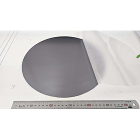
This is a cleaning sheet / reshaping sheet for probe pins of probe cards. Its unique self-repairing coating automatically closes holes created during touchdown, allowing for repeated use of the same area approximately 5 to 10 times (unlike typical competitor sheets, which leave holes after one use and require moving to unused areas). This reduces the surface area of the sheet used and the frequency of replacements, leading to lower maintenance costs. Our company, which possesses processing and evaluation technology for semiconductor testing probe pins, has jointly developed and manufactured this product with Towa Chemical Co., Ltd., a specialized manufacturer of silicone rubber molded products. The formulation of the abrasive can be adjusted according to the material of the target probe (such as P7, AgPdCu, Rh, Ir, rhenium tungsten, etc.), the tip shape, and the purpose of cleaning / reshaping. We offer two types: a wafer type for MEMS and vertical probe cards (directly installed onto the prober chuck) and a sheet type for cantilever and epitaxial probe cards (which can be cut to fit the equipment). *The number of uses may vary depending on the target probe and usage conditions. Please feel free to consult us first.
Inquire About This Product
basic information
【Wafer Type】Compatibility: MEMS and Vertical Type / Size: 200mm, 300mm / Installation: Directly installed on the prober chuck / Heat resistance temperature: 200°C / Total thickness: approximately 1mm 【Sheet Type】Compatibility: Cantilever and Epitaxial Type / Size: Can be cut to fit the equipment / Installation: Fixed to the stage with adhesive tape / Heat resistance temperature: 150°C Common Specifications: There are two types of products: cleaning and reshaping. The layer composition includes a silicone coating (self-repairing), abrasive (proprietary blend), and substrate (wafer type uses silicon wafers, sheet type uses silicon substrates and adhesive tape).
Price range
Delivery Time
Applications/Examples of results
The corresponding probe materials are P7, AgPdCu, Rh, Ir, rhenium tungsten, etc. Performance record: 5 to 10 uses at the same location (the general guideline for other companies' products is 1 use). After 100 touchdowns, no pinhole blockage was observed. Reshaping evaluation example: P7 φ0.076 2.5°T, OD amount 0.4mm, with a 62% reduction in tip diameter after 2000 touchdowns (from 18.65μm to 7.11μm).
Detailed information
-
Cleaning sheet type Forms a cleaning layer. Just touch down to remove dirt and debris from the pin tip.
-
The worn probe pin tip is precisely polished and shaped to restore inspection accuracy. Achieved a 62% reduction in tip diameter after 2,000 touch downs. High polishing power due to a unique three-layer structure.
-
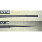
Reshaping evaluation example: P7 φ0.076 2.5°T, OD amount 0.4mm, with a 62% reduction in tip diameter (from 18.65μm to 7.11μm) after 2000 touch downs.
catalog(1)
Download All Catalogs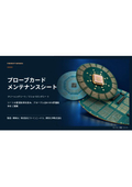
Company information

Our company specializes in the processing of various probe pins used in semiconductor testing. When striving to advance manufacturing, it is essential to develop both technology and skills in order to improve quality, shorten delivery times, and tackle new challenges. By continuously applying creativity and innovation to our technology and skills, we will meet our customers' needs and contribute to society.