Investment Analysis Information for Semiconductor Electrostatic Chucks 2026: Explaining the Growth Strategy to Reach a Scale of 1,434 Million USD.
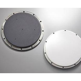
The global market for electrostatic chucks (ESC) for semiconductors is expected to expand from approximately 1.324 billion USD in 2025 to about 1.434 billion USD in 2026, with a compound annual growth rate (CAGR) of 5.8% from 2026 to 2032, reaching approximately 2.016 billion USD by 2032. The global production volume in 2025 is estimated to be around 57,485 units, with an average price of about 23,030 USD per unit, a production capacity of approximately 74,000 units, and an industry average gross profit margin of 39.8%. Electrostatic chucks for semiconductors are critical components that electrostatically hold wafers in front-end equipment such as PVD, PECVD, etching, EUV, and ion implantation, responsible for positioning and temperature control.
Inquire About This Product
basic information
Global Market Size of Electrostatic Chucks for Semiconductors According to the latest research report published by Global Reports titled "Global Market Size, Share, Company Rankings, Revenue, and Demand Trend Forecast for Electrostatic Chucks for Semiconductors (2026-2032)," the global market size for electrostatic chucks for semiconductors is expected to expand from approximately 1,324 million USD in 2025 to around 1,434 million USD in 2026. It is projected to continue growing at a compound annual growth rate (CAGR) of 5.8%, reaching approximately 2,016 million USD by 2032.
Price range
Delivery Time
Applications/Examples of results
The technological evolution and 300mm adaptation of electrostatic chucks for semiconductors Electrostatic chucks for semiconductors consist of a conductive base, an insulating layer, and electrodes, and they uniformly hold thin wafers using electrostatic force generated by applying voltage. In particular, in processes such as etching, film deposition, and ion implantation, the uniformity of temperature across the wafer surface, adhesion strength, detachment response, and plasma resistance are directly linked to process yield. With the miniaturization of advanced nodes and the widespread use of 300mm wafers, their positioning has shifted from mere clamping components to high-functionality materials that simultaneously support thermal management and process stability. The competitive axis for electrostatic chucks for semiconductors has also transitioned from the supply capacity of individual components to a comprehensive strength that includes materials, electrode structures, processing precision, surface treatment, and reliability evaluation. The thermal conductivity, plasma resistance, and dielectric properties vary by material, such as alumina, aluminum nitride (AlN), silicon carbide (SiC), and polyimide, and the choice between Coulomb-type and Johnsen-Rahbek (JR) type, as well as single-electrode, bipolar, and multi-electrode structures, also influences applications.
Company information

Global Reports integrates industrial information from around the world and provides highly accurate market intelligence to support corporate decision-making. We deliver in-depth analyses based on numerical data and facts, including market size, share, industry structure, price trends, growth forecasts, rankings of major companies, and competitive trends, with clear information categorized by country, region, and application. Leveraging a rich database that has supported the business growth of over 65,000 companies and an international research network, we accompany our clients in their global expansion and continuous growth.