DAF (Die Attach Film) market size 2026-2032: Significant expansion with a growth rate of 6.3%.
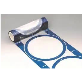
Die Attach Film (DAF) refers to the global market for Die Attach Film (DAF), which is expanding against the backdrop of thinner and more densely packed semiconductor packaging. The market size is expected to reach approximately \$320 million by 2025 and about \$339 million by 2026, with a compound annual growth rate (CAGR) of 6.3% from 2026 to 2032, predicting a market size of around \$489 million by 2032. The global production volume in 2025 is estimated to be 24.6 million units, with a production capacity of 30 million units, an average selling price of \$13 per unit, and a gross profit margin of 32%. DAF is a functional material that bonds chips to substrates, lead frames, or between stacked chips, supporting a wide range of applications including memory, logic, power semiconductors, and advanced packaging.
Inquire About This Product
basic information
Global Market Size of Die Attach Film (DAF) According to the latest research report published by Global Reports titled "Global Market Size, Share, Company Rankings, Sales, and Demand Trend Forecast for Die Attach Film (DAF) (2026-2032)", the global market size of die attach film (DAF) is expected to expand from approximately 320 million USD in 2025 to around 339 million USD in 2026. It is projected to continue growing at a compound annual growth rate (CAGR) of 6.3%, reaching approximately 489 million USD by 2032.
Price range
Delivery Time
Applications/Examples of results
Technical Requirements and Applications of Die Attach Film (DAF) Die Attach Film (DAF) is pre-attached to the back side of wafers and chips and is used in the chip bonding process after dicing. In thin packages and multi-chip stacked structures, in addition to adhesion strength, uniformity of film thickness, suppression of resin overflow, reduction of warpage, heat resistance, and long-term reliability are important. Furthermore, thermal conductivity, electrical properties, and compatibility with existing manufacturing processes are also required. Applications extend to memory devices, power semiconductors, RF devices, and chips for high-performance computing, as well as FC-BGA, wafer-level packaging (WLP), 3D packaging, and system-in-package (SiP). As chip thinning and multilayering progress, the optimization of DAF material design and bonding processes significantly affects product yield.
Company information

Global Reports integrates industrial information from around the world and provides highly accurate market intelligence to support corporate decision-making. We deliver in-depth analyses based on numerical data and facts, including market size, share, industry structure, price trends, growth forecasts, rankings of major companies, and competitive trends, with clear information categorized by country, region, and application. Leveraging a rich database that has supported the business growth of over 65,000 companies and an international research network, we accompany our clients in their global expansion and continuous growth.