Direct exposure device market size forecast 2026: Expected to reach 1,462 million USD by 2032.
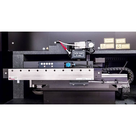
A direct-write exposure device is a machine that uses controllable energy beams such as lasers or electron beams to directly draw circuits or fine structures on a substrate coated with photoresist. It is suitable for small-batch production, prototyping, and accommodating design changes, as it can form patterns without the need for traditional photomasks. It is used in semiconductor research and development, MEMS, advanced packaging, display masks, microfluidic chips, and optoelectronic devices.
Inquire About This Product
basic information
Global Market Size of Direct Imaging Exposure Equipment According to the latest research report published by Global Reports titled "Global Market Size, Share, Company Rankings, Sales, and Demand Trend Forecast for Direct Imaging Exposure Equipment (2026-2032)," the global market for direct imaging exposure equipment is expanding against the backdrop of the densification of printed circuit boards (PCBs), advancements in semiconductor advanced packaging, and the sophistication of manufacturing technologies for next-generation displays. The market size is expected to increase from 890 million USD in 2025 to 958 million USD in 2026, growing at a compound annual growth rate (CAGR) of 7.3% from 2026 to 2032, and is projected to reach 1.462 billion USD by 2032. The global production volume in 2025 is estimated to be approximately 1,163 units, with an average market price of about 765,000 USD per unit.
Price range
Delivery Time
Applications/Examples of results
Direct Drawing Exposure Devices: Methods and Applications Direct drawing exposure devices are equipment that directly draw circuits and fine patterns onto photoresist using lasers or electron beams, eliminating the need for photomasks. They can be broadly classified into optical (laser) and charged particle types (electron and ion beams), with electron beam systems being particularly strong in producing IC masks that require precision on the order of about 10nm. Laser systems excel in productivity and are suitable for high-function PCBs, wafer-level packages, FPD masks, low-end IC front-end processes, and copper plating for solar cells. In PCBs, practical applications are advancing in multilayer boards, HDI, flexible substrates, and IC carrier substrates, while in large-scale production for semiconductor front-end processes, resolution and processing capability remain challenges.
Company information

Global Reports integrates industrial information from around the world and provides highly accurate market intelligence to support corporate decision-making. We deliver in-depth analyses based on numerical data and facts, including market size, share, industry structure, price trends, growth forecasts, rankings of major companies, and competitive trends, with clear information categorized by country, region, and application. Leveraging a rich database that has supported the business growth of over 65,000 companies and an international research network, we accompany our clients in their global expansion and continuous growth.