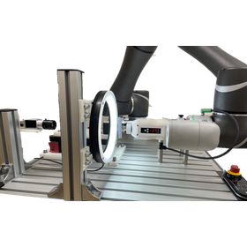
Achieves overwhelming high precision compared to general microscopic visual measurements! Enables short time and high reproducibility with a high-precision CMOS camera.
The "Lens Appearance Inspection Device" is an inspection device that achieves overwhelming high precision and high reproducibility in a short time compared to conventional microscope visual measurements. Equipped with a high-speed, high-resolution camera and an innovative lighting system, it performs automatic inspections simply by manually setting the sample, accommodating a wide range from individual lenses to modules. It can detect foreign objects, scratches, and cracks, and can easily be adapted for inline use. 【Features】 ■ High-speed, high-resolution camera and innovative lighting system ■ Supports inspection of both individual lenses and modules ■ Capable of inspecting foreign objects, scratches, cracks, etc. ■ Automatically executes inspections after sample loading ■ Easily adaptable for inline use *For more details, please download the PDF or feel free to contact us.

Inquire About This Product
basic information
【Specifications】 ■ Configuration: 12 million pixel CMOS camera, F-mount lens (2x magnification), LED transmitted surface lighting, individually lit LED ring light, computer for image processing, Camera Link image input board, motor controller board, LCD display ■ Pixel resolution: Approximately 2.75μ/pixel ■ Field of view size: Approximately 11mm x 8.25mm ■ Transmitted lighting size: 120mm x 100mm ■ Z-axis stroke: Approximately 10mm ■ Image processing functions: Brightness unevenness correction, automatic recognition of sample position, automatic binarization (binarization based on average brightness and offset), automatic appearance measurement (area average diameter, length of bounding rectangle) *For more details, please download the PDF or feel free to contact us.
Price range
Delivery Time
Applications/Examples of results
【Purpose】 ■Appearance inspection of small lenses (including smartphones) ■Inspection of both individual lenses and modules ■Inspection for foreign objects, scratches, cracks, etc. *For more details, please download the PDF or feel free to contact us.
catalog(1)
Download All Catalogs
Company information

Since our company's establishment in 1986, we have long been engaged in semiconductor-related businesses that support Japan's cutting-edge technology. On the hardware side, we have developed construction and manufacturing environments, including clean rooms. On the human resources side, we have focused on training semiconductor engineers and establishing a service system that can promptly respond to customer needs. Last year, we participated in SEMICON Japan for the first time, and by directly interacting with many industry stakeholders, we were able to learn again what is currently needed and what services should be created. At the same time, the morale within the company has been rising, and we are actively conducting sales activities. It is said that the Japanese economy is finally showing signs of recovery. However, even just looking at the semiconductor industry, the entry of overseas manufacturers and the significant improvement in technology and services are remarkable, so we aim to enhance our international competitiveness in our sales expansion. Not only domestically but also in response to the era of globalization, our role as a hub connecting North America and Asia, especially given our excellent airport access, will further increase.