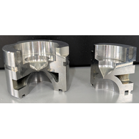
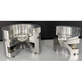
High-precision horizontal (wet) device for PCM and PCB.
Miniaturization Processing Capability (Fine Pattern & High Etching Factor) - PCB Field: Supports ultra-fine wiring width/wiring spacing (L/S = 15/15 μm or more) in line with the latest mSAP/Anylayer processes. - PCM Field: Ensures verticality and smoothness of fine holes and slit edges for stainless steel masks (FMM), lead frames, or microchannel plates, completely suppressing burrs (capillary defects and protrusions). Excellent In-Plane Uniformity (Uniformity Control): Independent inverter control/pressure regulation for upper and lower sprays: The injection pressure of the upper and lower sprays can be individually adjusted according to the thickness variation of the substrate and the pattern deviation.

Inquire About This Product
basic information
SKyline
Price range
Delivery Time
Applications/Examples of results
High-precision horizontal devices for PCM and PCB (wet process equipment for etching, developing, stripping, etc.) are widely used in modern industrial manufacturing, particularly in high-end fields. They are applied in the following two major areas: 1. PCB (Printed Circuit Board) and Semiconductor Packaging Field High-end substrate manufacturing (mSAP, Anylayer, HDI substrates, etc.): Etching, developing, and resist stripping of fine wiring in high-density interconnection substrates for smartphones, servers, and 5G communication devices. Achieving extremely narrow wiring widths and spacings (fine patterns) to meet the demands of chip packaging and highly integrated electronic devices. IC substrate manufacturing: Producing precision substrates necessary for the packaging of semiconductor chips, ensuring extremely high wiring accuracy and verticality of edges. 2. PCM (Photochemical Etching / Precision Metal Processing) Field Chemical etching is a "stress-free" process, which does not produce mechanical burrs or deformations, making this equipment widely used for the manufacturing of various high-precision, irregularly shaped metal parts with fine holes. Electronic and display components: New energy and automotive industry: Medical and optical equipment:
catalog(1)
Download All Catalogs
Company information

WorldLink Co., Ltd. Founded in 2022, WorldLink Co., Ltd. is a professional industrial agency based in Osaka, Japan. Founder Mr. Peter has 23 years of professional experience in the semiconductor, solar energy, lithium battery and automation industries. The company has signed official agency cooperation agreements with German enterprises TSK, Photonics-Systems-Group, Ekvip Automation and Chinese enterprise Beijing Nanotop electronic Technology. WorldLink focusing on providing partners with Japanese market development, business connection and localized operation services.