
Japan Mask-Free Exposure Equipment Industry Report 2026: Growth Outlook to Reach 945 Million USD
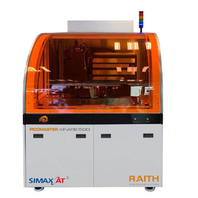
Global Market Size of Mask-Free Exposure Equipment According to the latest research report published by Global Reports titled "Global Market Size, Share, Company Rankings, Sales, and Demand Trend Forecast for Mask-Free Exposure Equipment (2026-2032)," the global market for maskless exposure equipment is expected to expand from approximately 709 million USD in 2025 to about 945 million USD in 2026, and reach around 2.72 billion USD by 2032. The compound annual growth rate (CAGR) from 2026 to 2032 is projected to be high at 19.1%. Maskless exposure equipment refers to exposure and drawing devices that directly form patterns on substrates using methods such as electron beams, lasers, digital optical projection, and focused ion beams, without the use of physical photomasks or reticles. Its importance is increasing in the semiconductor and microfabrication fields, where it can reduce the time and cost of mask production, making it suitable for low-volume production, prototyping, and design changes.
Inquire About This Product
basic information
Advanced packaging is driving the growth of digital exposure. Maskless exposure systems are expanding their applications from traditional prototype equipment for research and development to flexible manufacturing platforms that support advanced packaging, silicon photonics, quantum devices, MEMS, and biomedical devices. In particular, in the semiconductor sector for AI and HPC, technological advancements such as HBM, chiplets, FOWLP, PLP, and redistribution layers (RDL) require high-precision pattern formation on large substrates and rapid responses to process changes. Against this backdrop, digital maskless exposure is expected to be a key area driving market expansion in the future.
Price range
Delivery Time
Applications/Examples of results
Trends by Technology in EBL, DLW, and Digital Exposure Maskless exposure systems can be broadly categorized into electron beam lithography (EBL), direct laser writing (DLW), digital maskless exposure, and focused ion beam (FIB) lithography. EBL forms nanoscale fine patterns using a focused electron beam and can be divided into single Gaussian beam, variable shaped beam, and parallel multi-beam methods. In 2025, its market sales share was expected to be about 43.61%, making it the largest segment, but by 2032, digital maskless exposure is predicted to occupy about 43.13%, becoming the largest segment. DLW utilizes direct drawing and photopolymerization with lasers, accommodating grayscale structures, micro-optical components, microfluidic devices, and two-photon/multi-photon fabrication. Its market share in 2025 was approximately 18.34%. FIB lithography is responsible for processing, injection, film formation, and nano-patterning using focused ion beams, and while its market share in the same year was only about 4.93%, it has applications that are difficult to replace, such as processing quantum structures and special materials.
Company information
Global Reports integrates industrial information from around the world and provides highly accurate market intelligence to support corporate decision-making. We deliver in-depth analyses based on numerical data and facts, including market size, share, industry structure, price trends, growth forecasts, rankings of major companies, and competitive trends, with clear information categorized by country, region, and application. Leveraging a rich database that has supported the business growth of over 65,000 companies and an international research network, we accompany our clients in their global expansion and continuous growth.