
List of Semiconductor Manufacturing Equipment products
- classification:Semiconductor Manufacturing Equipment
211~225 item / All 5248 items


It won't break even after 1 million repetitions! A mat switch with reliable operation, high durability, and low price. Suitable for options in machine tools as well. Please consult us about delivery t...
- Sensors


We can accommodate high resistance over 10,000 ohms, with diameters ranging from approximately 30 mm to 8 inches, and we also offer thinning and chip processing arrangements!
- Other semiconductors
- Processing Contract
- Wafer


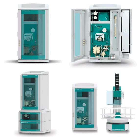
Quantification of anions in high-concentration sodium hydroxide solution for semiconductor manufacturing using ion chromatography.
- Wafer
- Analytical Equipment and Devices
- Semiconductor inspection/test equipment

Evaluation of Organic Coatings on Metals Using Electrochemical Measurement Devices Based on ISO 17463 - Paints and Varnishes
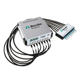
- Etching Equipment
- Wafer
- Other surface treatment equipment
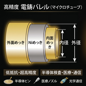

Achieving ultra-high precision that is difficult with cutting processes. By reducing resistance through inner and outer surface plating, we solve the challenges of extending the lifespan of semiconduc...
- Semiconductor inspection/test equipment


Seventeen years since the publication of the '21st Century Edition Handbook on Film Fabrication Applications,' we are releasing a new edition that solidifies the fundamentals while enhancing new appli...
- Technical and Reference Books
- Other surface treatment equipment
- Other semiconductor manufacturing equipment


We offer a lineup of electron beam lithography systems, ranging from high-precision types with an acceleration voltage of 100 kV to universal types with SEM functionality, capable of meeting various n...
- Electron beam lithography equipment
- Other surface treatment equipment
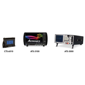

We will protect our customers' investments in legacy radios and support functional verification!
- Tester
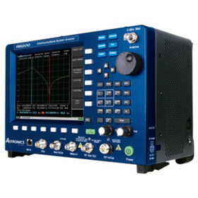
This is a test device that combines a wide range of digital tests and analog LMR tests!
- Tester
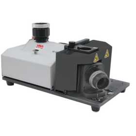

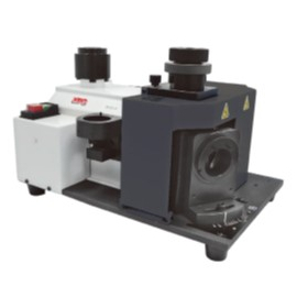
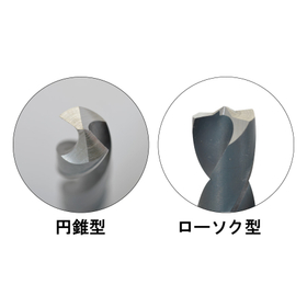
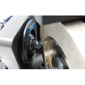
For those troubled by drill runout and cutting edge damage! Achieve improved processing accuracy and extended tool life with flat grinding methods.
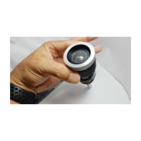
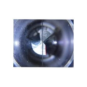
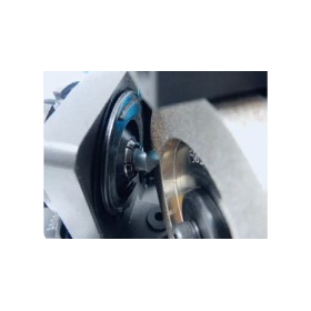
- Wafer processing/polishing equipment
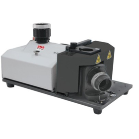
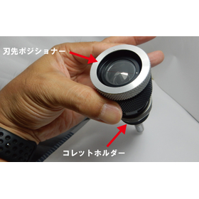
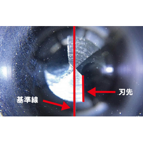
The adoption of a unique blade tip positioner and an adjustable collet holder allows for quick and accurate visual drill setup!
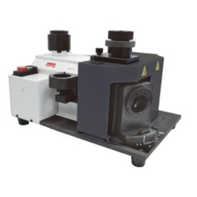
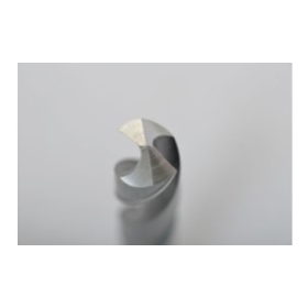
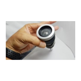
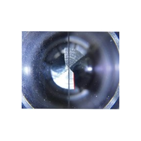
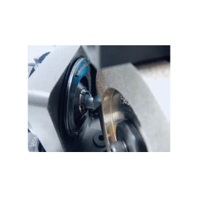
- Wafer processing/polishing equipment
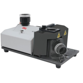
For those troubled by drill runout and cutting edge damage! Achieve improved processing accuracy and extended tool life with flat surface grinding methods.
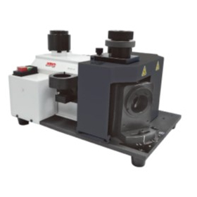
- Wafer processing/polishing equipment


Due to its modular embedded design, it is possible to flexibly assemble dedicated machines according to the required film formation methods. A compact thin-film experimental device that can accommodat...
- Sputtering Equipment
- Evaporation Equipment
- Annealing furnace

4-Yen Multi-Sputtering Device 【MiniLab-S060】
4 cathodes with Φ2 inch configuration Simultaneous film deposition: 3-component simultaneous deposition (RF 500W or DC 850W) + HiPIMS (PulseDC 5KW) x 1 Power distribution and configuration settings for 4 cathodes can be freely changed via the HMI screen using the plasma relay switch 3 MFC systems (Ar, O2, N2) for reactive sputtering RIE etching stage RF 300W (main chamber) + <30W soft etching (LL chamber) Substrate heating: Max 500℃, 800℃, or 1000℃ (C/C or SiC coating) Substrate rotation and vertical movement (automatically controlled by stepping motor) APC automatic control: Upstream (MFC flow adjustment) or downstream (automatic valve opening adjustment on the exhaust side) Dimensions: 1,120(W) x 800(D) ● Mixed specifications for resistance heating deposition, organic material deposition, EB deposition, PECVD, etc. are also possible.

◉ Short time: Easily conduct graphene synthesis experiments in just 30 minutes per batch. ◉ High-precision temperature and pressure control. ◉ Sophisticated software.
- CVD Equipment

VOXIA compact X-ray CT imaging device
Compact design with a space-saving layout that can be installed anywhere. Despite its compact body, it generates high-resolution data through advanced calculation software. * X-ray tube voltage: 20-90kV, or 40-maximum 130kV * Focus diameter: 7μm (5μm@4W) * Detector pixel: 89μm, approximately 3.2 million pixels! * Sample size: Φ120mm ◉ Vcap (Control Software): A custom-made imaging stage tailored to the subject and purpose. A series of tasks from shooting to image output can be performed with just a click. High-speed continuous shooting in as fast as 20 seconds, with processing from shooting start to image reconstruction taking about 30 seconds. ◉ VCT (Reconstruction Software): Customizable automatic measurement and analysis software specialized for the specified subject. High-speed reconstruction of shooting data with 992 x 992 pixel images and 600 projections in just 3.8 seconds! ◉ MolcerPlus (3D Display Analysis): Custom software that enables measurement conditions that were difficult with conventional software. Software for displaying, processing, and measuring the imaged object. ● High safety, ● Compatible with a wide variety of samples, ● Intuitive HMI, easy operation.