
List of Semiconductor Manufacturing Equipment products
- classification:Semiconductor Manufacturing Equipment
1126~1170 item / All 5250 items


It won't break even after 1 million repetitions! A mat switch with reliable operation, high durability, and low price. Suitable for options in machine tools as well. Please consult us about delivery t...
- Sensors


We can accommodate high resistance over 10,000 ohms, with diameters ranging from approximately 30 mm to 8 inches, and we also offer thinning and chip processing arrangements!
- Other semiconductors
- Processing Contract
- Wafer


Achieving thin film coating in micrometer units with a coater head (slot coat) application device.
- Coater

Used for temporary fixing and bonding with hot melt adhesive!
- Molding Equipment


We provide high-quality circuit processing and wiring processing services using FIB. We achieve a high processing yield!
- Semiconductor inspection/test equipment
- Semiconductors and ICs
- Microcomputer

Supply disruptions from semiconductor manufacturers, the electrification of the automotive industry, and the spread of 5G communication. Are you keeping up with the urgent need for alternative product evaluations, authenticity assessments, and failure analysis?
The spread of 5G communication, the electrification of the automotive industry, the intensification of US-China trade friction represented by certain semiconductor manufacturers leading to supply stoppages, and the rapid increase in digital products due to the impact of the COVID-19 pandemic are various social phenomena that are increasing the demand for semiconductors. Along with these developments, the acceleration of semiconductor supply risks is progressing. In addition to the adoption of new products, evaluation of existing and distributed products is also necessary... However, the personnel involved in new adoption and product evaluation are limited. Do you have any of these concerns? - Lack of know-how to evaluate semiconductor components - Want to evaluate alternative products but lack personnel and equipment - Want to use stock items and market products but have concerns about reliability - Unable to determine whether the delivered semiconductor products are counterfeit or genuine At Eurofins FQL, we leverage our years of experience in component evaluation and failure analysis to provide not only semiconductor evaluations but also failure analysis services. Additionally, we offer evaluations of distributed products to assist in determining the authenticity of counterfeit, imitation, or long-term stored items. Please feel free to contact us.


Processing S45C quenched and tempered steel using high-precision CNC machining technology. Manufacturing ring components for semiconductor manufacturing equipment.
- Other semiconductor manufacturing equipment
- Processing Contract

Using SUS304 stainless steel and utilizing NC lathes, machining centers, and cylindrical grinding, we manufacture high-precision ring components for semiconductor manufacturing equipment.
- Other semiconductor manufacturing equipment
- Processing Contract


Handling electronic assembly products such as solder balances and stirrers, as well as soldering equipment and semiconductor devices!
- Soldering Equipment
- Other semiconductor manufacturing equipment


Inspection is possible only on the surface of the double-sided implementation substrate! Also compatible with 3D tomography inspection. *Detailed explanatory materials will be provided.
- Semiconductor inspection/test equipment
- X-ray inspection equipment

Automatically inspect crystal defect voids inside silicon wafers!
- Semiconductor inspection/test equipment
- X-ray inspection equipment

X-ray observation device for analysis with a high resolution of 0.25 μm focal spot size.
- Semiconductor inspection/test equipment
- X-ray inspection equipment

Automated X-ray inspection device for inspecting solder bumps on wafers.
- Semiconductor inspection/test equipment
- X-ray inspection equipment
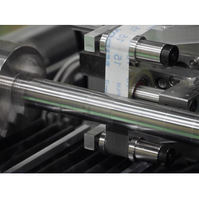

Automation of super finishing processes and uniformity of roughness. We propose polishing equipment for outer diameter, inner diameter, end face, etc., tailored to your applications and shapes.
- Wafer processing/polishing equipment


Highly versatile! Guarantees a shining edge, perfect finish, and short processing time.
- Wafer processing/polishing equipment

A highly versatile fully electric solution for flat and shaped edges!
- Wafer processing/polishing equipment

Guaranteed high-quality finish and consistent performance! Stone grinding machine with excellent output.
- Wafer processing/polishing equipment
- Stone Processing Machinery

Vivid in the vertical direction! Precisely vertically polished straight edges of marble and granite.
- Wafer processing/polishing equipment

Unique solutions for precision, efficiency, and reliability in stone polishing.
- Wafer processing/polishing equipment
- Stone Processing Machinery


High-precision inspection equipment compatible with transparent materials.
- Semiconductor inspection/test equipment

[Exhibition Information] We will be exhibiting at 'SEMICON JAPAN 2025'.
We will be exhibiting Kubota's semiconductor inspection equipment at SEMICON JAPAN, an international exhibition of manufacturing technologies, equipment, and materials in the semiconductor industry. All of our staff sincerely look forward to your visit. 【Exhibition Information】 Date: December 17 (Wed) - 19 (Fri), 2025, 10:00 - 17:00 Venue: Tokyo Big Sight Booth Location: W1963 *Advance registration is required for attendance. Please check the SEMICON JAPAN website for registration details.

Automating visual inspection of wafer defects.
- Semiconductor inspection/test equipment
[Exhibition Information] We will be exhibiting at 'SEMICON JAPAN 2025'.
We will be exhibiting Kubota's semiconductor inspection equipment at SEMICON JAPAN, an international exhibition of manufacturing technologies, equipment, and materials in the semiconductor industry. All of our staff sincerely look forward to your visit. 【Exhibition Information】 Date: December 17 (Wed) - 19 (Fri), 2025, 10:00 - 17:00 Venue: Tokyo Big Sight Booth Location: W1963 *Advance registration is required for attendance. Please check the SEMICON JAPAN website for registration details.

Equipped with a review microscope! Defects detected can be observed in real-time with the microscope.
- Semiconductor inspection/test equipment
[Exhibition Information] We will be exhibiting at 'SEMICON JAPAN 2025'.
We will be exhibiting Kubota's semiconductor inspection equipment at SEMICON JAPAN, an international exhibition of manufacturing technologies, equipment, and materials in the semiconductor industry. All of our staff sincerely look forward to your visit. 【Exhibition Information】 Date: December 17 (Wed) - 19 (Fri), 2025, 10:00 - 17:00 Venue: Tokyo Big Sight Booth Location: W1963 *Advance registration is required for attendance. Please check the SEMICON JAPAN website for registration details.


Tabletop conveyor. How about for simple verification of fine parts?
- Image Processing Equipment
- Other semiconductor manufacturing equipment

3D Inspection Device HISR - Assisting with precise inspection and verification.


- Color camera
- Other semiconductor manufacturing equipment


We have achievements such as 'sputtering equipment with GB for organic EL' and 'IBS equipment for research and development'!


- Sputtering Equipment

We have a track record of equipment such as 'plasma CVD systems for metal containers' and 'ICP-type MOCVD systems'!


- CVD Equipment

Supports tray transport! Achieves excellent substrate temperature distribution and gas flow method.

- Annealing furnace
- Heating device

Switching between RIE mode and DP mode is possible! Reduction of metal contamination through special surface treatment.
- Etching Equipment

Reduction of particles through suitable surface treatment! Compatible with high vacuum processes using a load-lock system.
- Evaporation Equipment

We have a track record of devices such as the "two-stage composite Pt deposition system"! Please contact us when you need assistance.


- Evaporation Equipment

You can freely choose from the plasma cleaning chamber, organic deposition chamber, electrode deposition chamber, sealing chamber, and more!


- Evaporation Equipment

Maximum substrate heating temperature of 1000℃! Reduces element loss specific to the substrate surface heating process!

- Heating device
- Annealing furnace

It is a versatile and compact device that enables etching, ashing, and ion cleaning!
- Etching Equipment
- Ashing device

Demo units available for loan! Ideal for spin drying silicon wafers, masks, and film substrates!
- Other clean room equipment and facilities
- Other semiconductor manufacturing equipment

Demo units available for loan! This is a cassette-type batch cleaning device that can accommodate up to Φ300.
- Other semiconductor manufacturing equipment

Demo units available for loan! This is a sheet-type cleaning device that can accommodate up to Φ300.
- Other semiconductor manufacturing equipment

Demo units available for loan! This is a device that performs a series of cleaning and etching processes, including pure water treatment and drying.
- Etching Equipment

【Demo unit available for loan!】A semi-automatic device that transports wafers from the processing tank to the rinse tank via an arc.
- Etching Equipment

Demo units available for loan! Wafers are loaded and processed in a dedicated barrel.
- Etching Equipment

Demo units available for loan! After pre-processing with a cassette, automatic etching is performed with a dedicated barrel.
- Etching Equipment

Demo units available for loan! A clean filter is installed at the top to ensure cleanliness within the chamber.
- Other semiconductor manufacturing equipment

Demo units available for loan! We offer a variety of options including batch type and scrub cleaning.
- Other semiconductor manufacturing equipment

Demo units available for loan! We will accommodate according to the shape of the quartz tube, so please consult with us.
- Other semiconductor manufacturing equipment

Possible at 10,000 rpm with a compact small option!
- Coater
- Other semiconductor manufacturing equipment

Target work: Applicable to 2"□ to 5"□ substrates or φ2" to φ5" substrates!
- Coater
- Other semiconductor manufacturing equipment

Technology has been incorporated to achieve a uniform high-precision coating!
- Coater
- Other semiconductor manufacturing equipment