
List of Semiconductor Manufacturing Equipment products
- classification:Semiconductor Manufacturing Equipment
1981~2025 item / All 5250 items


It won't break even after 1 million repetitions! A mat switch with reliable operation, high durability, and low price. Suitable for options in machine tools as well. Please consult us about delivery t...
- Sensors


We can accommodate high resistance over 10,000 ohms, with diameters ranging from approximately 30 mm to 8 inches, and we also offer thinning and chip processing arrangements!
- Other semiconductors
- Processing Contract
- Wafer


"Best Washing" does not discriminate against dirt. It is a powerful detergent that is gentle on the environment, versatile in use, and a completely new high-performance detergent.
- Resist Device
- Etching Equipment


Orte's collet accommodates a variety of colorful advanced shapes. Unique and complex designs and machining are also possible!

- Other semiconductor manufacturing equipment


Removable test lead! Equipped with a tote band meter that can withstand a 1m drop.
- Tester

Flexibly respond to the manufacturer's discontinuation of bonding products.

- Bonding Equipment


For educational institutions and small facilities! A desktop system that allows for easy operation with a touch panel.
- Etching Equipment


Achieve fast deep learning for object detection, image classification, and feature extraction!
- Business Intelligence and Data Analysis
- Image analysis software
- Semiconductor inspection/test equipment


The cross-section of electronic components is simple and finishes beautifully!!
- Wafer processing/polishing equipment
- Other abrasives


Automatic insertion of all probe pins. Exchange of any specified pins is also possible.
- Tester
- Semiconductor inspection/test equipment


The number of output channels and other output signals can also be customized according to your requests!
- Ammeter
- Testing Equipment and Devices
- Semiconductor inspection/test equipment


Compact yet high-performance. Compatible with a wide range of processes.
- Other semiconductor manufacturing equipment
- Heating device

Catalog < Thank You for Visiting SEMICON J! >
Thank you very much for visiting our booth at SEMICON J 2022 at the end of last year. Under the concept of "Partner@yourFab," we introduced a wide range of solutions. With your support, we were able to conclude the event successfully and smoothly. We sincerely appreciate it. We have prepared the product catalog that was distributed during the event as a digital file. We hope you find it useful.
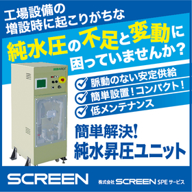
The pure water pressure shortage and its fluctuations due to the expansion of factory facilities are resolved by the pure water booster unit! It ensures a stable supply.
- Other semiconductor manufacturing equipment
- Flow Control
Catalog < Thank You for Visiting SEMICON J! >
Thank you very much for visiting our booth at SEMICON J 2022 at the end of last year. Under the concept of "Partner@yourFab," we introduced a wide range of solutions. With your support, we were able to conclude the event successfully and smoothly. We sincerely appreciate it. We have prepared the product catalog that was distributed during the event as a digital file. We hope you find it useful.


It is a compactly designed manual auto-alignment exposure device (mask aligner).
- Other semiconductor manufacturing equipment

Fully automatic exposure device (mask aligner) compatible with Ø2” to 6”
- Other semiconductor manufacturing equipment

Exposure device (mask aligner) compatible with Ø200mm and Ø300mm.
- Other semiconductor manufacturing equipment


High-frequency cleaning machines suitable for precision cleaning (500kHz, 1MHz) ---- <<Test machine rental (for a fee), please contact us>>
- Other semiconductor manufacturing equipment


Introducing services that meet a wide range of needs, such as product structure verification! Useful for defective product analysis.
- Semiconductor inspection/test equipment
- Analysis Services
- LED Module

Comparing the heat dissipation characteristics of different materials! Introducing a case study of transient thermal resistance measurement.
- Semiconductor inspection/test equipment
- Circuit board design and manufacturing
- LED Module


Anode bonding device
- Hydraulic Equipment
- Granulating Equipment
- Other semiconductor manufacturing equipment


Package removal without causing physical or electrical damage! High selectivity etching.
- Etching Equipment
- Ultrasonic Cleaner
- Drying Equipment

Equipped with a flow management system! Processing of powders at high temperatures using CVD/PECVD is possible.
- CVD Equipment

Various plasma sources can be equipped! Customized design for CVD, MOCVD, and ALD equipment.
- CVD Equipment

Minimize radioactive contamination! Capable of proposing plasma excitation technology tailored to specific applications.
- Ion implantation equipment


We propose fine processing technology for next-generation package substrates using KrF excimer lasers!
- Other semiconductor manufacturing equipment

Metal, dielectric, and organic film deposition! Introducing the thermal evaporation device.
- Evaporation Equipment

The maximum film-forming temperature is 800°C! It can accommodate up to 4x DLI evaporators with the chamber heating mechanism.
- CVD Equipment

Due to lamp heating, RTP and RTCVD processing is possible! Quartz tube-type chamber.
- Annealing furnace

Turbo pump compatible! Low temperature (1100°C) / high temperature (1300°C) pyrometer.
- Annealing furnace

Supports a maximum substrate size of 156mm x 156mm! Compatible with vacuum or atmospheric transport systems and can be equipped with a load lock.
- Annealing furnace

Rapid cooling mechanism after annealing! Introducing the high-speed heat treatment equipment from Annealsys.
- Annealing furnace

Compatible with SI 500-1M, SI 500 PPD-1M, etc.! The transport chamber is available in three types.
- CVD Equipment

Control of ion density by ICP power! Achieving low-temperature film formation, low damage, and high conformality.
- CVD Equipment

High-selectivity etching! Optimization of radical supply by adjusting the spacing between the ICP source and the substrate electrode.
- Other semiconductor manufacturing equipment

Top-class throughput! Flexible modular design.
- Other semiconductor manufacturing equipment

Many safety measures specifications necessary for mass production! Compact device size with a film formation temperature of 50 to 285°C.
- Other semiconductor manufacturing equipment

500℃ wafer stage! Adoption of a remote ICP source with no plasma damage.
- Other semiconductor manufacturing equipment

For research and development, for small-scale batches! Standard equipped with a simple decontamination unit ALD Shield Vapor Trap.
- Other semiconductor manufacturing equipment

Substrate bias mechanism! Introducing our microwave PECVD/etching equipment.
- Etching Equipment

Introducing the ion beam sputtering device equipped with a maximum of 5 targets (220mm diameter) or 4 targets (300mm diameter)!
- Sputtering Equipment

Maximum 200mm diameter substrate! Double ring magnetron (Fraunhofer FEP)
- Sputtering Equipment

Mechanical clamp or electrostatic chuck compatible! Sub-nanometer etching mechanism.
- Etching Equipment

Supports wafers up to 150 or 200 mm! Etching angle and stage tilt/rotation mechanism.
- Etching Equipment


Interlock covers are also available! We have achieved further efficiency in polishing operations.
- Wafer processing/polishing equipment
- Other processing machines

Ideal for sample preparation for research and development! Successfully reduced vibration and noise significantly.
- Wafer processing/polishing equipment
- Other processing machines

High-precision angular bearings are adopted as the main axis! Achieving a flatness accuracy of ±10μm on the reference table.
- Wafer processing/polishing equipment
- Other processing machines