
List of Semiconductor Manufacturing Equipment products
- classification:Semiconductor Manufacturing Equipment
136~180 item / All 5250 items


It won't break even after 1 million repetitions! A mat switch with reliable operation, high durability, and low price. Suitable for options in machine tools as well. Please consult us about delivery t...
- Sensors


We can accommodate high resistance over 10,000 ohms, with diameters ranging from approximately 30 mm to 8 inches, and we also offer thinning and chip processing arrangements!
- Other semiconductors
- Processing Contract
- Wafer
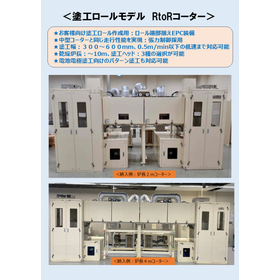

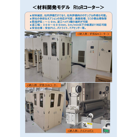
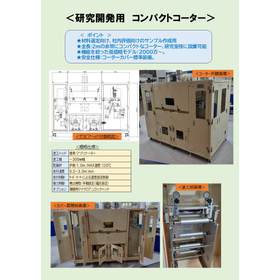
Small-scale test coater for material development using RtoR (Roll-to-Roll) technology.
- Coater
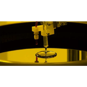

Mass production support and small batch production support! A system that automatically handles the series of processes for resist coating, baking, and cooling.
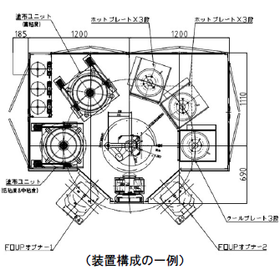
- Resist Device
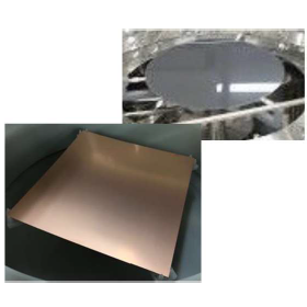
Introducing a system that automatically processes each step from stripping, rinsing, to spin drying!
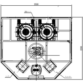
- Resist Device

Compatible with 2 to 12-inch wafers. Customizable for each item.
- Other cleaning machines
- Other semiconductor manufacturing equipment
- Other semiconductors
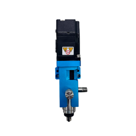

Ideal for precise application of high-viscosity thermal conductive gel materials!
- Other semiconductor manufacturing equipment
- dispenser

Continuously measure the target circuits of the material supply process. By comparing production plans, material changes, setup, work records, and current history, you can confirm usage trends.
- Sensors
- Other semiconductor manufacturing equipment
- Instrumentation and Control Systems
Collect simple measurement data from multiple single-phase three-wire and three-phase three-wire circuits. Organize it by line, equipment group, and period, and it can be confirmed on a common screen.
- Sensors
- Injection Molding Machine
- Other semiconductor manufacturing equipment


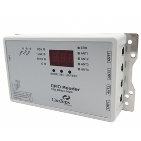
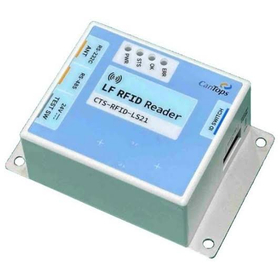
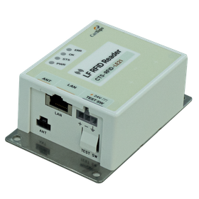
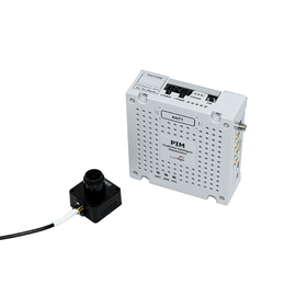
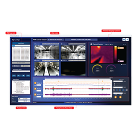
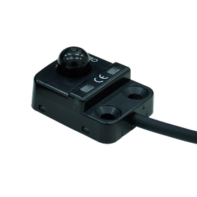
Total solution provided from equipment development stage to line operation! Operates stably in a light noise environment.
- Other semiconductor manufacturing equipment
Compare the use of existing PLCs, small-scale cloud solutions, and centralized management through monitoring software. You can choose a configuration that matches the scale of implementation, verifica...
- Other machine tools
- Other processing machines
- Other semiconductor manufacturing equipment
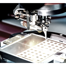

Options to prevent stoppage in the subsequent processes that cannot be halted.
- Other semiconductor manufacturing equipment


Explanation of specialized terms in grinding and polishing.
- Wafer processing/polishing equipment


PUR hot melt applicator
- Molding Equipment
- glue
- Other packaging machines
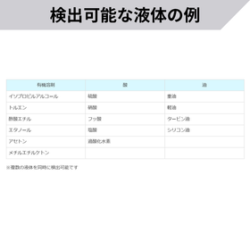
![[Leak Detection] An algorithm for n...](https://image.mono.ipros.com/public/product/image/315214/IPROS12853703792727575734.PNG?w=280&h=280)

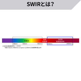
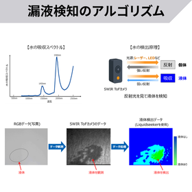
[Leakage Prevention] Not a single drop of leakage will be overlooked without touching. Move to liquid leakage monitoring without tape.
- Business Intelligence and Data Analysis
- Other measurement, recording and measuring instruments
- Other semiconductor manufacturing equipment

Notice of Participation in the 'Hokuyou Bank Manufacturing Sustainability Fair'
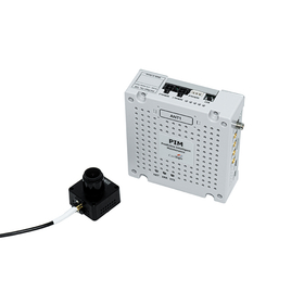
We are pleased to announce that we will be exhibiting at the "Hokuyo Bank Manufacturing Sustainability Fair" to be held on July 22, 2026 (Wednesday) at Access Sapporo. We would like to invite you to visit us at this opportunity. <Exhibition Overview> Name: Hokuyo Bank Manufacturing Sustainability Fair Date: July 22, 2026 (Wednesday) Venue: Access Sapporo, Booth Number 86 <Exhibited Products> ■ Energy-saving Wireless Mesh Network NetNucleus LPWA We will introduce a solution that easily realizes the collection and visualization of monitoring data from manufacturing equipment using wireless devices powered by AA batteries. ■ Wind Direction and Speed IoT Sensor anemolink-2D We will showcase a wind direction and speed meter that allows for easy visualization and data collection of wind direction and speed in environments such as semiconductor clean rooms. ■ Liquid Leak Detection Algorithm Liquidseeker We will present a technology that detects liquid leaks non-contact, contributing to reduced maintenance costs by eliminating issues such as disconnection and peeling compared to traditional leak detection tape.
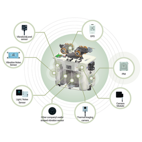
You can monitor the equipment and conditions in the factory in real time!
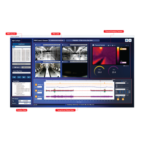
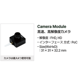
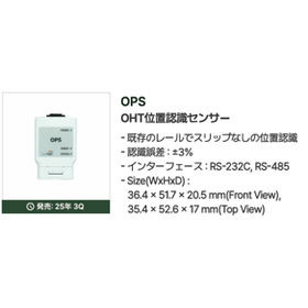
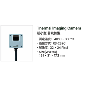
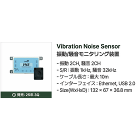
- Other semiconductor manufacturing equipment
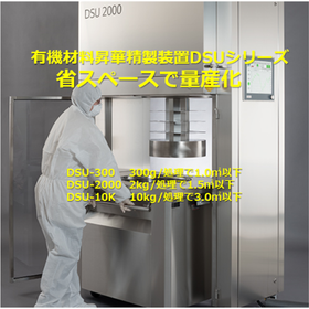

Achieving both high purity and high yield. Contributing to the purification of semiconductor materials.
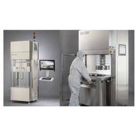
- Other semiconductor manufacturing equipment
- Refining and Extraction Equipment
- Organic EL
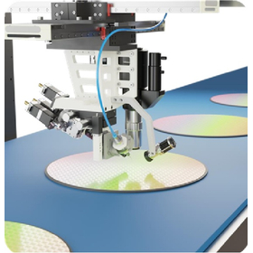

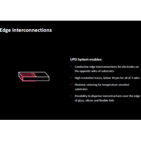
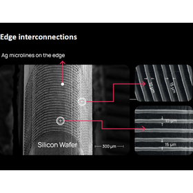
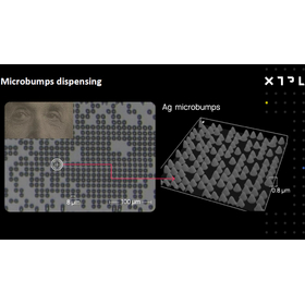
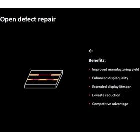
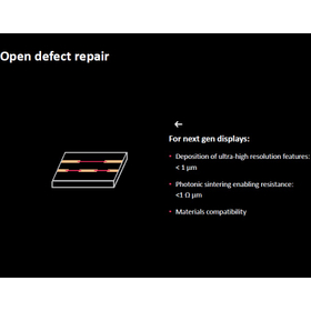
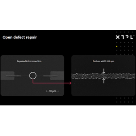
A dispenser that can draw lines of 1 micron!
- dispenser
- Other semiconductor manufacturing equipment


Max 1000℃, MFC maximum 3 systems, APC pressure control, compatible with 4" or 6" substrates, high vacuum annealing equipment (<5 × 10^-7 mbar)
- Annealing furnace
- Heating device
- Electric furnace
VOXIA compact X-ray CT imaging device
Compact design with a space-saving layout that can be installed anywhere. Despite its compact body, it generates high-resolution data through advanced calculation software. * X-ray tube voltage: 20-90kV, or 40-maximum 130kV * Focus diameter: 7μm (5μm@4W) * Detector pixel: 89μm, approximately 3.2 million pixels! * Sample size: Φ120mm ◉ Vcap (Control Software): A custom-made imaging stage tailored to the subject and purpose. A series of tasks from shooting to image output can be performed with just a click. High-speed continuous shooting in as fast as 20 seconds, with processing from shooting start to image reconstruction taking about 30 seconds. ◉ VCT (Reconstruction Software): Customizable automatic measurement and analysis software specialized for the specified subject. High-speed reconstruction of shooting data with 992 x 992 pixel images and 600 projections in just 3.8 seconds! ◉ MolcerPlus (3D Display Analysis): Custom software that enables measurement conditions that were difficult with conventional software. Software for displaying, processing, and measuring the imaged object. ● High safety, ● Compatible with a wide variety of samples, ● Intuitive HMI, easy operation.

A compact multi-thin film device that incorporates sputtering, deposition, electron beam (EB), and annealing thin film modules in a 60-liter volume chamber, suitable for various applications.
- Sputtering Equipment
- Evaporation Equipment
- CVD Equipment

MiniLab-WCF Ultra High Temperature Wafer Annealing Furnace Max 2000℃_Dedicated for High-Temperature Wafer Sintering (6inch to 8inch)
Max 2000℃ Φ6〜8 inch wafer dedicated high-temperature annealing device, capable of small-scale production multi-atmosphere wafer annealing device. ◾️ Max 2000℃ ◾️ Effective heating range: Φ6〜Φ8 inch single wafer type or batch type (multi-stage 5 wafer cassette) ◾️ Heater control: 1 zone or 2 zones (cascade control) ◾️ Heater materials: ・C/C composite: Φ6〜Φ8 inch ・PG coating high-purity graphite: Φ6〜Φ8 inch ◾️ Operating atmosphere: ・Vacuum (1x10⁻²Pa), inert gas (Ar, N2) ◾️ PLC semi-automatic operation ・Automatic sequence control for vacuum/purge cycle and venting ・Fully automatic operation (optional) ・Touch panel operation, allowing centralized management without dispersed operations. ◾️ Process pressure control ・APC control (MFC flow or automatic opening adjustment valve PID loop control) ・Maximum 3 systems of MFC flow automatic control, or manual adjustment of float meter/needle valve ◾️ PLOT screen graph display, CSV data output

Flexible configuration available upon request for methods such as deposition, sputtering, and EB. Adopts a tall chamber with a height of 570mm, contributing to improved uniformity during deposition.
- Evaporation Equipment
- Sputtering Equipment
- Etching Equipment

4-Yen Multi-Sputtering Device 【MiniLab-S060】
4 cathodes with Φ2 inch configuration Simultaneous film deposition: 3-component simultaneous deposition (RF 500W or DC 850W) + HiPIMS (PulseDC 5KW) x 1 Power distribution and configuration settings for 4 cathodes can be freely changed via the HMI screen using the plasma relay switch 3 MFC systems (Ar, O2, N2) for reactive sputtering RIE etching stage RF 300W (main chamber) + <30W soft etching (LL chamber) Substrate heating: Max 500℃, 800℃, or 1000℃ (C/C or SiC coating) Substrate rotation and vertical movement (automatically controlled by stepping motor) APC automatic control: Upstream (MFC flow adjustment) or downstream (automatic valve opening adjustment on the exhaust side) Dimensions: 1,120(W) x 800(D) ● Mixed specifications for resistance heating deposition, organic material deposition, EB deposition, PECVD, etc. are also possible.

Compact and space-saving! Ideal for research and development, flexible configuration for purposes such as deposition, sputtering, and annealing.
- Evaporation Equipment
- Sputtering Equipment
- Annealing furnace
4-Yen Multi-Sputtering Device 【MiniLab-S060】
4 cathodes with Φ2 inch configuration Simultaneous film deposition: 3-component simultaneous deposition (RF 500W or DC 850W) + HiPIMS (PulseDC 5KW) x 1 Power distribution and configuration settings for 4 cathodes can be freely changed via the HMI screen using the plasma relay switch 3 MFC systems (Ar, O2, N2) for reactive sputtering RIE etching stage RF 300W (main chamber) + <30W soft etching (LL chamber) Substrate heating: Max 500℃, 800℃, or 1000℃ (C/C or SiC coating) Substrate rotation and vertical movement (automatically controlled by stepping motor) APC automatic control: Upstream (MFC flow adjustment) or downstream (automatic valve opening adjustment on the exhaust side) Dimensions: 1,120(W) x 800(D) ● Mixed specifications for resistance heating deposition, organic material deposition, EB deposition, PECVD, etc. are also possible.
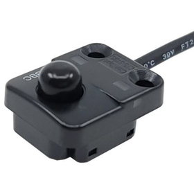
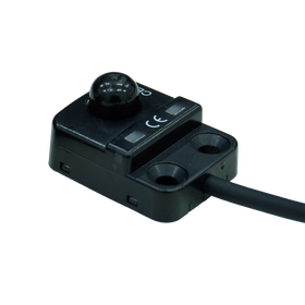
Stable detection unaffected by light noise is possible with contact sensors! Designed for over 10 million high durability cycles.
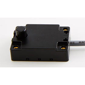
- Other semiconductor manufacturing equipment
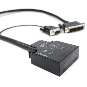
World's first! Wireless E84 sensor
- Other semiconductor manufacturing equipment


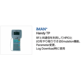
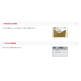
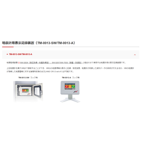
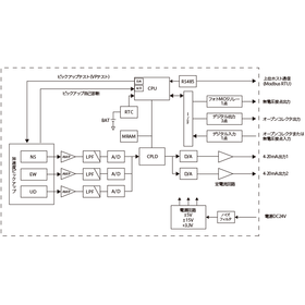
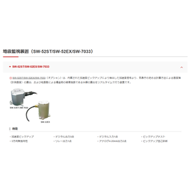
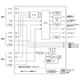
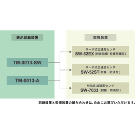
Up to 3 earthquake monitoring devices can be connected.
- Other machine tools
- Semiconductor inspection/test equipment
- Metal bearings


We are a problem-solving company that realizes "visualization" of energy conservation and measurement!
- Other measurement, recording and measuring instruments
- Sensors
- Tester


Achieving high-quality polishing that preserves the edge through automation.
- Wafer processing/polishing equipment

We will exhibit at the SURTECH 2025 trade show.
We will be exhibiting at SURTECH 2025 – Surface Technology Exhibition – which will be held at Tokyo Big Sight from January 29, 2025 (Wednesday). We will introduce the "DLyte," a dry electrochemical polishing machine that uses resin media for ion exchange to grind and polish metals. Exhibition: SURTECH 2025 Location: Tokyo Big Sight, East Hall 3 Organizer: JTB Communication Design, Inc. (Rapid News Publications Ltd.) Date: January 29 (Wednesday) to January 31 (Saturday), 2025 Time: 10:00 AM to 5:00 PM Booth Number: 3X-11 *For inquiries and to download the catalog, please visit here. You can find more detailed information on our website. Request for materials: https://www.nttdata-xam.com/document/ Inquiries: https://www.nttdata-xam.com/contact/

Achieving high-quality polishing that preserves edges through mechanization.
- Wafer processing/polishing equipment
We will exhibit at the SURTECH 2025 trade show.
We will be exhibiting at SURTECH 2025 – Surface Technology Exhibition – which will be held at Tokyo Big Sight from January 29, 2025 (Wednesday). We will introduce the "DLyte," a dry electrochemical polishing machine that uses resin media for ion exchange to grind and polish metals. Exhibition: SURTECH 2025 Location: Tokyo Big Sight, East Hall 3 Organizer: JTB Communication Design, Inc. (Rapid News Publications Ltd.) Date: January 29 (Wednesday) to January 31 (Saturday), 2025 Time: 10:00 AM to 5:00 PM Booth Number: 3X-11 *For inquiries and to download the catalog, please visit here. You can find more detailed information on our website. Request for materials: https://www.nttdata-xam.com/document/ Inquiries: https://www.nttdata-xam.com/contact/

Achieving high-quality polishing that retains the edge through mechanization.
- Wafer processing/polishing equipment
We will exhibit at the SURTECH 2025 trade show.
We will be exhibiting at SURTECH 2025 – Surface Technology Exhibition – which will be held at Tokyo Big Sight from January 29, 2025 (Wednesday). We will introduce the "DLyte," a dry electrochemical polishing machine that uses resin media for ion exchange to grind and polish metals. Exhibition: SURTECH 2025 Location: Tokyo Big Sight, East Hall 3 Organizer: JTB Communication Design, Inc. (Rapid News Publications Ltd.) Date: January 29 (Wednesday) to January 31 (Saturday), 2025 Time: 10:00 AM to 5:00 PM Booth Number: 3X-11 *For inquiries and to download the catalog, please visit here. You can find more detailed information on our website. Request for materials: https://www.nttdata-xam.com/document/ Inquiries: https://www.nttdata-xam.com/contact/

Achieving high-quality polishing that preserves edges through mechanization.
- Wafer processing/polishing equipment
We will exhibit at the SURTECH 2025 trade show.
We will be exhibiting at SURTECH 2025 – Surface Technology Exhibition – which will be held at Tokyo Big Sight from January 29, 2025 (Wednesday). We will introduce the "DLyte," a dry electrochemical polishing machine that uses resin media for ion exchange to grind and polish metals. Exhibition: SURTECH 2025 Location: Tokyo Big Sight, East Hall 3 Organizer: JTB Communication Design, Inc. (Rapid News Publications Ltd.) Date: January 29 (Wednesday) to January 31 (Saturday), 2025 Time: 10:00 AM to 5:00 PM Booth Number: 3X-11 *For inquiries and to download the catalog, please visit here. You can find more detailed information on our website. Request for materials: https://www.nttdata-xam.com/document/ Inquiries: https://www.nttdata-xam.com/contact/

Achieving high-quality polishing that preserves the edge through mechanization.
- Wafer processing/polishing equipment
We will exhibit at the SURTECH 2025 trade show.
We will be exhibiting at SURTECH 2025 – Surface Technology Exhibition – which will be held at Tokyo Big Sight from January 29, 2025 (Wednesday). We will introduce the "DLyte," a dry electrochemical polishing machine that uses resin media for ion exchange to grind and polish metals. Exhibition: SURTECH 2025 Location: Tokyo Big Sight, East Hall 3 Organizer: JTB Communication Design, Inc. (Rapid News Publications Ltd.) Date: January 29 (Wednesday) to January 31 (Saturday), 2025 Time: 10:00 AM to 5:00 PM Booth Number: 3X-11 *For inquiries and to download the catalog, please visit here. You can find more detailed information on our website. Request for materials: https://www.nttdata-xam.com/document/ Inquiries: https://www.nttdata-xam.com/contact/
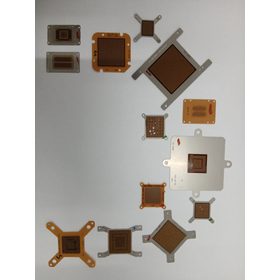

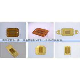
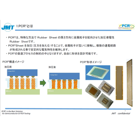
A sheet socket that enables stable inspection in semiconductor back-end process inspection! What is "PCR" that allows for high-speed and high-density measurements? Technical materials on operating pri...
- Other electronic parts
- socket
- Semiconductor inspection/test equipment
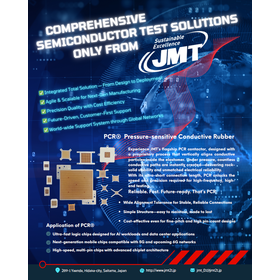
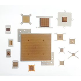
Test solution that does not damage solder balls or measurement substrates with soft contact!
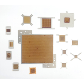
- Semiconductor inspection/test equipment
- Printed Circuit Board