We have compiled a list of manufacturers, distributors, product information, reference prices, and rankings for microscope.
ipros is IPROS GMS IPROS One of the largest technical database sites in Japan that collects information on.

microscope(afm) - List of Manufacturers, Suppliers, Companies and Products

Last Updated: Aggregation Period:Sep 17, 2025~Oct 14, 2025
This ranking is based on the number of page views on our site.

microscope Product List

46~60 item / All 65 items

Displayed results

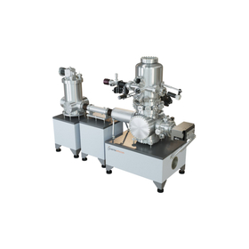
Microsphere-based super-resolution optical microscope with a resolution of ≦100nm.

Optical microscope with a resolution of ≦100nm, capable of non-destructive observation in full color.

It is possible to observe beyond the diffraction limit with spatial resolution below 100nm, allowing for non-destructive, full-color observation of nanoscale structures. It can be used for semiconductor research and development, as well as advanced material imaging, or as an alternative to SEM and AFM. The objective lens can also be sold separately.

  • Optical microscope

Added to bookmarks

Bookmarks list

Bookmark has been removed

Bookmarks list

You can't add any more bookmarks

By registering as a member, you can increase the number of bookmarks you can save and organize them with labels.

Free membership registration

Compact Type Atomic Force Microscope NaioAFM

Introducing a low-cost "All-in-one" AFM device that is compact, durable, and easy to operate!

"NaioAFM" is a compact atomic force microscope suitable for users who want to measure surface shapes concisely and quickly in the fields of nanotechnology education at universities and vocational schools, as well as in research and development or quality control. With the product's unique "Flip-over" scan head and dedicated exchange tools, it allows for quick and simple cantilever replacement. Balancing functionality and operability, it is an "All-in-one" AFM device that can be used by anyone, anywhere, and is widely utilized around the world. 【Features】 ■ Integrated controller, XY stage, wind shield, and vibration isolation mechanism ■ Equipped with a high-resolution top-view optical camera for positioning and side-view observation ■ Additional measurement modes can be added according to needs ■ Simple cantilever replacement: no need to adjust the laser or detector ■ Ready for measurement immediately after installation: just connect the USB cable and launch the software *For more details, please refer to the PDF document or feel free to contact us.

  • image_82.png
  • image_85.png
  • image_87.png
  • image_88.png
  • Other microscopes

Added to bookmarks

Bookmarks list

Bookmark has been removed

Bookmarks list

You can't add any more bookmarks

By registering as a member, you can increase the number of bookmarks you can save and organize them with labels.

Free membership registration

[PFM] Piezoelectric Response Microscope

By using a probe coated with a conductive film and applying an alternating voltage to the sample surface, the sample surface is vibrated to obtain electromechanical information.

- Visualization of attraction and repulsion due to the electric dipole effect of piezoelectric samples is possible. - Quantitative evaluation of the sample's expansion and contraction due to piezoelectric response is a reference value. - AFM images can also be obtained simultaneously.

  • Contract measurement

Added to bookmarks

Bookmarks list

Bookmark has been removed

Bookmarks list

You can't add any more bookmarks

By registering as a member, you can increase the number of bookmarks you can save and organize them with labels.

Free membership registration

[Analysis Case] Evaluation of Surface Roughness of SiC Trench MOSFET Trench Sidewalls

Quantitative evaluation of the roughness of trench sidewalls related to device characteristics.

In recent years, SiC has been attracting attention as a material for high-voltage devices. The trench MOSFET structure is necessary for the high integration of devices, and the application development for SiC devices is progressing. Since the channel region of the trench MOSFET structure is the trench sidewall, the flatness of the trench sidewall is related to the reliability of the device. This document introduces an example of quantitatively evaluating the roughness of the trench sidewall of SiC trench MOSFETs using AFM (Atomic Force Microscopy).

  • Contract Analysis
  • Other semiconductors

Added to bookmarks

Bookmarks list

Bookmark has been removed

Bookmarks list

You can't add any more bookmarks

By registering as a member, you can increase the number of bookmarks you can save and organize them with labels.

Free membership registration

[MFM] Magnetic Force Microscopy Method

MFM is a measurement technique that uses a probe coated with a magnetic film to measure the leakage magnetic field occurring near the sample surface and obtain magnetic information.

- Qualitative information on the magnetic properties of the sample can be obtained. - Imaging of attraction and repulsion due to leakage magnetic fields is possible. - A signal of magnetic force proportional to the magnitude of the gradient of the leakage magnetic field can be obtained, but quantitative evaluation is not possible. - AFM images can also be obtained simultaneously.

  • Contract Analysis

Added to bookmarks

Bookmarks list

Bookmark has been removed

Bookmarks list

You can't add any more bookmarks

By registering as a member, you can increase the number of bookmarks you can save and organize them with labels.

Free membership registration

LT STM (Low Temperature Scanning Tunneling Microscope)

Introduction to Scanning Tunneling Microscopy in Ultra-Low Temperature Environments

LT STM (Low Temperature Scanning Tunneling Microscope) refers to a scanning tunneling microscope operating in a cryogenic environment. It is a device with a proven sales record, capable of STM measurements at temperatures below 5K. 【Applications】 STM observation and measurement in the nano region under low temperature conditions. 【Features】 ● Increased hold time to >65h at the same performance level ● High frequency wiring ● Increased spectroscopy resolution ● Record proven platform since 1996 with more than 200 devices installed ● Reliable design ensuring high up-time ● Independent tip and sample temperature ● Leading QPlus AFM technology

  • Analytical Equipment and Devices

Added to bookmarks

Bookmarks list

Bookmark has been removed

Bookmarks list

You can't add any more bookmarks

By registering as a member, you can increase the number of bookmarks you can save and organize them with labels.

Free membership registration

[Data] Application Note: Life Sciences Edition

Consolidated on page 24! Introducing solutions related to pharmaceuticals, cosmetics, and bioimaging.

In this document, we will introduce how it contributes to advanced research and development, such as the visualization of biological structures and the development and manufacturing of pharmaceuticals and cosmetics. [Contents (Excerpt)] ■ Introduction ■ Evaluation of the chemical properties of pharmaceuticals and correlation techniques using confocal Raman microscopy ■ Analysis examples in the cosmetics field using AFM ■ Measurement of fluoride content in toothpaste ■ Bioimaging *Application note: Life Sciences edition available for free! Please download the PDF to view it. Feel free to contact us.

  • Other microscopes

Added to bookmarks

Bookmarks list

Bookmark has been removed

Bookmarks list

You can't add any more bookmarks

By registering as a member, you can increase the number of bookmarks you can save and organize them with labels.

Free membership registration

[Analysis Case] Evaluation of Ion Implantation Damage Layer in Gallium Oxide Ga2O3

Confirming the differences due to variations in annealing conditions after ion implantation.

Gallium oxide (Ga2O3) has a wider bandgap than SiC and GaN, and possesses excellent physical properties, making it a focus of attention as a material for power devices that can be expected to be high-efficiency and low-cost. Controlling impurity concentration and crystallinity, which influence the characteristics of the devices, is crucial for their development. This document presents the results of observations of the damage layer and changes in surface roughness caused by disturbances in the crystal structure due to ion implantation, under various annealing conditions. Measurement methods: TEM, AFM Product fields: Oxide semiconductors, power devices Analysis objectives: Shape evaluation, structural evaluation For more details, please download the document or contact us.

  • img_C0718_1.jpg
  • Contract Analysis
  • Contract measurement

Added to bookmarks

Bookmarks list

Bookmark has been removed

Bookmarks list

You can't add any more bookmarks

By registering as a member, you can increase the number of bookmarks you can save and organize them with labels.

Free membership registration

[SMM] Scanning Microwave Microscopy Method

Scanning Microwave Microscopy

SMM scans the measurement sample using a conductive probe to observe its surface topography. Simultaneously, microwaves are irradiated from the probe to the sample, and by measuring the reflected response, it is possible to obtain signals correlated with carrier concentration, particularly in the case of semiconductors. The intensity of the SMM signal is linearly correlated with carrier concentration, which is a characteristic feature that provides high quantitativeness. - For Si devices, sensitivity is present for carrier concentrations around 10^15 to 10^20 cm^-3. - Since signals correlated linearly with carrier concentration can be obtained, quantitative evaluation (semi-quantitative) is possible under certain assumptions. - AFM images can also be acquired. - Various semiconductors such as Si, SiC, GaN, InP, and GaAs can be measured. This document introduces application examples, principles, and data examples. For more details, please download the document or contact us.

  • 打ち合わせ.jpg
  • セミナー.jpg
  • Contract Analysis
  • Contract measurement
  • Contract Inspection

Added to bookmarks

Bookmarks list

Bookmark has been removed

Bookmarks list

You can't add any more bookmarks

By registering as a member, you can increase the number of bookmarks you can save and organize them with labels.

Free membership registration

ARCTIC SPM Lab

New type low-temperature scanning probe microscope

Redefining Low-Temperature SPM: A Closed-Cycle System Equipped with High Magnetic Field and Optical System Experience a new type of low-temperature scanning probe microscope with precision, efficiency, and adaptability. The ARCTIC SPM Lab features continuous operation, a compact footprint, and modular expandability to meet evolving research needs. Closed-cycle cooling technology enables a sustainable and cost-effective approach, eliminating dependence on helium. The SPM maintains excellent mechanical stability while providing virtually unlimited measurement time.

  • Other microscopes

Added to bookmarks

Bookmarks list

Bookmark has been removed

Bookmarks list

You can't add any more bookmarks

By registering as a member, you can increase the number of bookmarks you can save and organize them with labels.

Free membership registration

[New Release!] Atomic Force Microscope 'Park NX7'

[Japanese Version Catalog Available] New products with low cost, high functionality, and short delivery times! Introducing the atomic force microscopes we handle!

The "Park NX7" is equipped with all the new technologies developed by Park Systems and is available at an affordable price. This product is designed down to the finest details, just like the higher-end models, and can facilitate research. Additionally, it offers flat orthogonal XY scanning without bowing. Please feel free to contact us if you have any inquiries. 【Features】 ■ Highly expandable AFM solution ■ Flat orthogonal XY scanning without bowing ■ Low noise Z detector ■ Improved chip lifespan, sample preservation, and repeatability through True Non Contact mode * You can download the English version of the catalog. * For more details, please refer to the PDF materials or feel free to contact us.

  • Other microscopes

Added to bookmarks

Bookmarks list

Bookmark has been removed

Bookmarks list

You can't add any more bookmarks

By registering as a member, you can increase the number of bookmarks you can save and organize them with labels.

Free membership registration

[Document] Application Note: Battery Material Analysis Edition

Consolidated into a single application note! Introducing evaluation and analysis solutions that accelerate the development and quality control of battery materials.

This document introduces various application examples of how the evaluation of material properties with correlations can contribute to improving throughput across research, manufacturing, and the entire supply chain. It provides abundant information on topics such as "Measurement of grain size and microstructure of NCM cathode materials" and "Research on lithium-ion batteries using Raman correlation RISE microscopy." 【Contents (excerpt)】 ■ Introduction ■ Battery Applications ■ From Mines to Factories ■ ESM Measurement of Conductive Materials in Lithium-Ion Secondary Batteries ■ Desktop Multi-Nuclear NMR for Electrolyte Design *【Document】Application Note: Battery Material Analysis Edition is available for free! Please download the PDF to view it. Feel free to contact us.

  • Secondary Cells/Batteries

Added to bookmarks

Bookmarks list

Bookmark has been removed

Bookmarks list

You can't add any more bookmarks

By registering as a member, you can increase the number of bookmarks you can save and organize them with labels.

Free membership registration

[Data] Case Study of Material System Analysis

It is possible to prepare sections ranging from 30nm to 5μm! This document introduces several case studies of material analysis!

This document is a collection of case studies summarizing material analysis conducted by Hanai Corporation's Electron Microscope Technology Research Institute. The "Ultra Microtome" is suitable for producing high-quality ultra-thin sections and cross-sections across a wide range of fields, including biological tissues, metal plating layers, inorganic deposition layers, and nanoparticles. Our company has started offering contract analysis services. We will conduct material analysis in collaboration with partner organizations. [Published Cases] - Structural analysis of liposomes - Structural analysis of HIPS - Structural analysis of lens cross-sections - Cross-sectional observation of candy bags - Morphological observation of metal particles using the dispersion method (metal microparticles/metal-supported carbon) *For more details, please refer to the PDF document or feel free to contact us.

  • Contract Analysis
  • Electron microscope
  • Other microscopes

Added to bookmarks

Bookmarks list

Bookmark has been removed

Bookmarks list

You can't add any more bookmarks

By registering as a member, you can increase the number of bookmarks you can save and organize them with labels.

Free membership registration

3D Confocal Laser Raman Microscope Confotec NR500

High-end model: A top-level micro-Raman spectrometer with high sensitivity, high wavenumber resolution, and high expandability.

【Features】 - High spatial resolution: XY < 300 nm, Z < 600 nm (@532 nm) - High frequency resolution - High-speed imaging mode: Galvano scan 1000x1000 pixels/3 seconds - Automation features: Laser output, beam diameter, pinhole size, grating switching, etc. - High expandability: CARS model, AFM Raman/TERS, fluorescence lifetime measurement, autofocus function, SERS substrates, etc. - Low-frequency Raman measurement option - Brillouin scattering measurement option The device, equipped with a series of optical configurations such as a confocal pinhole, can automatically switch between them, enabling spectral analysis of micro-particles or Raman imaging of macro objects with high spatial resolution. It is a Raman microscope with a rich array of additional options and excellent expandability.

  • Laser microscope
  • Spectroscopic Analysis Equipment
  • Analytical Equipment and Devices

Added to bookmarks

Bookmarks list

Bookmark has been removed

Bookmarks list

You can't add any more bookmarks

By registering as a member, you can increase the number of bookmarks you can save and organize them with labels.

Free membership registration

Atomic Force Microscope "Handy AFM"

A super compact AFM with a depth and width that can take you anywhere, both measuring 15 cm.

The atomic force microscope "Handy AFM" can be used as a substitute for high-magnification optical microscopes. It features standard measurement modes, including static force mode, dynamic force mode, phase contrast, phase measurement, force modulation, spreading resistance, and external input capabilities. The scanning head is available in two types: high-resolution and wide-area, and they can be exchanged instantly. Probe replacement takes only a few seconds, and no adjustments are needed after replacement. Additionally, carbon nanotube probes can also be approached automatically. By using an electromagnetic scanner (patented) for scanning, there is no need to move the workpiece during the scan. Generally, it does not exhibit the non-linear creep or aging changes associated with piezo devices commonly used in AFMs. Optionally, it can be combined with a compact automatic stage. For more details, please download the catalog.

  • Electron microscope

Added to bookmarks

Bookmarks list

Bookmark has been removed

Bookmarks list

You can't add any more bookmarks

By registering as a member, you can increase the number of bookmarks you can save and organize them with labels.

Free membership registration