
High Heat Resistance and Low Loss All-LCP Flexible Substrate for 5G Communication
Flexible substrates with high heat resistance and low loss that support high-speed communication.
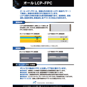
In the 5G communication industry, components with excellent high-frequency characteristics are required to achieve high-speed data transmission. It is particularly important to minimize signal transmission loss and ensure stable communication quality. Conventional substrates may face challenges with losses in the high-frequency range. Our high-heat-resistant, low-loss all-LCP flexible substrates utilize low dielectric constant materials to reduce losses of high-frequency signals, contributing to the acceleration of 5G communication. 【Application Scenarios】 - Base stations - High-speed data communication devices - High-frequency circuits 【Benefits of Implementation】 - Stabilization of high-speed data communication - Reduction of signal loss - Improvement of communication quality
- Company:山下マテリアル
- Price:Other


![[For Defense] High Heat Resistance and Low Loss All LCP Flexible Circuit Board](https://image.mono.ipros.com/public/product/image/2027794/IPROS16590387900970144219.jpg?w=280&h=280)


