We have compiled a list of manufacturers, distributors, product information, reference prices, and rankings for Electron microscope.
ipros is IPROS GMS IPROS One of the largest technical database sites in Japan that collects information on.

Electron microscope Product List and Ranking from 15 Manufacturers, Suppliers and Companies | IPROS GMS

Last Updated: Aggregation Period:Jul 08, 2026~Aug 04, 2026
This ranking is based on the number of page views on our site.

Electron microscope Manufacturer, Suppliers and Company Rankings

Last Updated: Aggregation Period:Jul 08, 2026~Aug 04, 2026
This ranking is based on the number of page views on our site.

  1. アイテス Shiga//Electronic Components and Semiconductors
  2. ロンビック Mie//Resin/Plastic
  3. 一般財団法人材料科学技術振興財団 MST Tokyo//Testing, Analysis and Measurement
  4. 4 大同分析リサーチ Aichi//Service Industry
  5. 5 花市電子顕微鏡技術研究所 Aichi//Service Industry

Electron microscope Product ranking

Last Updated: Aggregation Period:Jul 08, 2026~Aug 04, 2026
This ranking is based on the number of page views on our site.

  1. Observation of Cellulose Nanofibers (CNF) - Examples of SEM and TEM Observations ロンビック
  2. Crack observation using a tabletop SEM (scanning electron microscope). アイテス
  3. Comparison of cross-sectional observation images アイテス
  4. Examples of observing plastics and resin materials using TEM and SEM. ロンビック
  5. 5 [Case Analysis] Hepatocytes (Pig Liver) 花市電子顕微鏡技術研究所

Electron microscope Product List

31~55 item / All 55 items

Displayed results

[Data] Case Study of Material System Analysis

It is possible to prepare sections ranging from 30nm to 5μm! This document introduces several case studies of material analysis!

This document is a collection of case studies summarizing material analysis conducted by Hanai Corporation's Electron Microscope Technology Research Institute. The "Ultra Microtome" is suitable for producing high-quality ultra-thin sections and cross-sections across a wide range of fields, including biological tissues, metal plating layers, inorganic deposition layers, and nanoparticles. Our company has started offering contract analysis services. We will conduct material analysis in collaboration with partner organizations. [Published Cases] - Structural analysis of liposomes - Structural analysis of HIPS - Structural analysis of lens cross-sections - Cross-sectional observation of candy bags - Morphological observation of metal particles using the dispersion method (metal microparticles/metal-supported carbon) *For more details, please refer to the PDF document or feel free to contact us.

  • Contract Analysis
  • Electron microscope
  • Other microscopes
  • Electron microscope

Added to bookmarks

Bookmarks list

Bookmark has been removed

Bookmarks list

You can't add any more bookmarks

By registering as a member, you can increase the number of bookmarks you can save and organize them with labels.

Free membership registration

[Case Analysis] Hepatocytes (Pig Liver)

Insert photo ×7,000 Analysis of the cell membrane (×100,000)! It can be seen that the cell membrane has a double structure approximately 7nm wide.

We would like to introduce a case study of the analysis of 'hepatocytes (pig liver)' conducted by our company. The liver has many functions, including lipid and protein synthesis, metabolism and removal of drugs, and energy storage, most of which are composed of hepatocytes. There are also other components such as bile canaliculi (BC) and blood vessels (HS), within which blood cells (EC, Kf) can be observed. The inserted photo shows an enlargement of the cell membranes of adjacent cells, revealing that each cell membrane has a double structure approximately 7nm wide. Additionally, hepatocytes possess typical organelles that are often referenced when explaining the structure and function of general cells. [Analysis Overview] ■ Analysis Subject: Hepatocytes (pig liver) ■ It is evident that each cell membrane has a double structure approximately 7nm wide. ■ Hepatocytes have typical organelles that are frequently cited when explaining the structure and function of general cells. *For more details, please refer to the PDF document or feel free to contact us.

  • Contract Analysis
  • Electron microscope

Added to bookmarks

Bookmarks list

Bookmark has been removed

Bookmarks list

You can't add any more bookmarks

By registering as a member, you can increase the number of bookmarks you can save and organize them with labels.

Free membership registration

Basic Analysis Methods for Things that are Similar Yet Different

Introducing the flow from optical microscope observation with a wide range of applications to SEM observation and EDX elemental analysis!

We will introduce the flow from basic and widely applicable optical microscope observation to SEM observation and EDX elemental analysis. Observation using an optical microscope is one of the fundamental observation techniques, allowing for quick examination of general shapes and other features. Its advantage lies in the ability to obtain color information, making it effective for observing abnormalities associated with corrosion and other changes. In this document, we also provide detailed explanations of "observation using SEM" and "elemental analysis using EDX" with the help of photos and graphs. We encourage you to read it. [Contents] ■ Observation using an optical microscope ■ Observation using SEM ■ Elemental analysis using EDX *For more details, please refer to the PDF document or feel free to contact us.

  • image_02.png
  • image_03.png
  • image_04.png
  • image_05.png
  • image_06.png
  • Other contract services
  • Electron microscope

Added to bookmarks

Bookmarks list

Bookmark has been removed

Bookmarks list

You can't add any more bookmarks

By registering as a member, you can increase the number of bookmarks you can save and organize them with labels.

Free membership registration

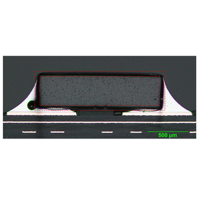
Comparison of cross-sectional observation images

We will introduce suitable observation methods for cross-sectional observation of chip resistors and copper wiring sections!

To assist you in selecting an observation device, we will introduce the differences in visibility between a metal microscope, W-SEM, and FE-SEM. When observing the cross-section of a chip resistor, certain areas may be difficult to observe at low magnification with a metal microscope, but with SEM observation, the greater depth of field allows for high-flatness images even at low magnification. When observing the cross-section of copper wiring, the copper-resin interface and the condition inside cracks can be observed with W-SEM, but with FE-SEM, even the crystal grains and tiny voids at the connection interface can be clearly observed. [Comparison] ■ Cross-section observation of chip resistors: Comparison of images between metal microscope and W-SEM ■ Cross-section observation of copper wiring: Comparison of images between W-SEM and FE-SEM *For more details, please download the PDF or feel free to contact us.

  • Other microscopes
  • Electron microscope

Added to bookmarks

Bookmarks list

Bookmark has been removed

Bookmarks list

You can't add any more bookmarks

By registering as a member, you can increase the number of bookmarks you can save and organize them with labels.

Free membership registration

[Analysis Case] Visualization of Strain at Heterojunction Interfaces in Compounds

Lattice image analysis using the FFTM method

The Fast Fourier Transform Mapping method is a technique that performs a Fourier transform on high-resolution TEM images to analyze and visualize the minute lattice distortions of crystals from the spot positions of the FFT pattern. Through FFTM analysis, it is possible to (1) analyze lattice distortions in the x and y directions of the image, (2) analyze lattice distortions in the crystal plane direction, (3) analyze the distribution of crystal plane spacing and crystal plane orientation, (4) display the data distribution as a histogram, and (5) detect distortions of 0.5% with a spatial resolution of 5 nm. An example of its application to compound heterojunction multilayer film samples is presented.

  • InGaP_GaAs多層膜の高分解能TEM像.png
  • FFTサイズの設定.png
  • FFTパターン.png
  • Contract Analysis
  • Electron microscope

Added to bookmarks

Bookmarks list

Bookmark has been removed

Bookmarks list

You can't add any more bookmarks

By registering as a member, you can increase the number of bookmarks you can save and organize them with labels.

Free membership registration

[Analysis Case] Preprocessing Technology for Specific Areas of Wafers and Chips

We will sample only the target area and produce samples without breaking the wafer.

We will extract small pieces from the wafer chip without breaking it and thin them down for high-resolution TEM observation and analysis. Furthermore, by cutting and preparing samples while leaving the areas to be analyzed, we will conduct TEM observation and analysis of the target areas from any desired direction and provide the data. Through advanced TEM sample preparation techniques, we will meet various observation, analysis, and evaluation needs.

  • Contract Analysis
  • Electron microscope

Added to bookmarks

Bookmarks list

Bookmark has been removed

Bookmarks list

You can't add any more bookmarks

By registering as a member, you can increase the number of bookmarks you can save and organize them with labels.

Free membership registration

[Analysis Case] Evaluation of the Diffusion Layer of Power Transistors (DMOSFET)

You can understand the positional relationship between the gate layer, source layer, and body layer.

We investigated the shape and positional relationship of the poly-Si gate, n-type source layer, and p-type body layer of commercially available power transistors (DMOSFETs). By overlaying AFM images, we can also understand the positional relationship with the gate.

  • Contract Analysis
  • Electron microscope

Added to bookmarks

Bookmarks list

Bookmark has been removed

Bookmarks list

You can't add any more bookmarks

By registering as a member, you can increase the number of bookmarks you can save and organize them with labels.

Free membership registration

[Analysis Case] Evaluation of pn Junction and Grain Structure of CIGS Film

Electron beam induced current method and crystal orientation analysis using SEM.

CIGS thin-film polycrystalline solar cells are expected to be low-cost next-generation solar cells. Development is underway for large-area and high-quality production. To evaluate the characteristics of the polycrystalline thin film, we conducted assessments of the pn junction using EBIC and crystal grain evaluation using EBSD on the same cross-section. We prepared a cross-section of the CIGS film and measured the open-circuit voltage (EBIC) by scanning an electron beam, visualizing the in-plane distribution of the open-circuit voltage. Additionally, by measuring EBSD on the same surface, we correlated the distribution of the open-circuit voltage with the crystal grains.

  • SEM.png
  • EBIC.png
  • Contract Analysis
  • Electron microscope

Added to bookmarks

Bookmarks list

Bookmark has been removed

Bookmarks list

You can't add any more bookmarks

By registering as a member, you can increase the number of bookmarks you can save and organize them with labels.

Free membership registration

[Analysis Case] Evaluation of Crystal Grains in CIGS Film

Crystal orientation analysis using SEM.

CIGS thin-film polycrystalline solar cells are being developed as next-generation solar cells expected to achieve low cost, large area, and high quality, and crystal information is required in this process. The EBSD method allows for the evaluation of crystal grains in CIGS films. The crystal information obtained from the EBSD method mainly includes orientation and grain size.

  • Contract Analysis
  • Electron microscope

Added to bookmarks

Bookmarks list

Bookmark has been removed

Bookmarks list

You can't add any more bookmarks

By registering as a member, you can increase the number of bookmarks you can save and organize them with labels.

Free membership registration

[Analysis Case] Structural Observation of the Hall Side Wall ONO Film

Planar TEM observation of specific areas using the FIB method.

By using FIB technology that allows for processing at the nanoscale, it is possible to perform planar TEM observations of specific areas. This enables the confirmation of the ONO three-layer structure (silicon oxide film / silicon nitride film / silicon oxide film) of the capacitor insulating film on the sidewall of the hole, which is difficult to verify through cross-sectional observations.

  • Contract Analysis
  • Electron microscope

Added to bookmarks

Bookmarks list

Bookmark has been removed

Bookmarks list

You can't add any more bookmarks

By registering as a member, you can increase the number of bookmarks you can save and organize them with labels.

Free membership registration

[Analysis Case] Evaluation of the Structure and Dispersion of Microparticles in Liquid

Observation of cross-sectional structure of liquid samples using cryo-SEM.

When evaluating the particle size and structure of fine particles dispersed in a liquid, conventional methods involved drying the liquid to extract the fine particles as a powder, which were then measured using an electron microscope. However, this method was not suitable for investigating how fine particles are actually dispersed in the liquid used. Therefore, we will introduce a case where cryo-processing and SEM observation were performed to directly evaluate how fine particles are dispersed within a liquid sample.

  • Contract Analysis
  • Electron microscope

Added to bookmarks

Bookmarks list

Bookmark has been removed

Bookmarks list

You can't add any more bookmarks

By registering as a member, you can increase the number of bookmarks you can save and organize them with labels.

Free membership registration

[Analysis Case] Evaluation of Electrode Materials for Lithium-Ion Secondary Batteries

Cross-sectional observation using atmosphere-controlled ion polishing (IP) processing is possible.

The electrodes of lithium-ion secondary batteries are very significant constituent materials that greatly influence the performance and reliability of the battery, such as its capacity. By performing ion polishing (IP) processing on the electrode materials after charge-discharge cycle testing under controlled atmospheric conditions, we can accurately observe them while minimizing degradation due to atmospheric exposure. In this instance, we will present a case that verifies the effect of atmospheric control on the positive electrode materials of lithium-ion secondary batteries after charge-discharge cycles by comparing the results of SEM observations after IP processing.

  • Contract Analysis
  • Contract measurement
  • Electron microscope

Added to bookmarks

Bookmarks list

Bookmark has been removed

Bookmarks list

You can't add any more bookmarks

By registering as a member, you can increase the number of bookmarks you can save and organize them with labels.

Free membership registration

[Analysis Case] Evaluation of Crystal Defects in SiC Power Devices Using PL and TEM

High-resolution TEM observation of crystal defects detected by PL mapping.

In PL (photoluminescence) mapping, it is possible to identify the positions of crystal defects from the luminescent areas. Furthermore, by performing high-resolution STEM observation (HAADF-STEM images) at the same locations, we can capture stacking defects. In this case study, we investigated commercially available SiC power devices using PL mapping and STEM. After identifying the positions of stacking defects through PL mapping, we conducted μ-sampling at the defect edge and performed cross-sectional STEM observation.

  • Contract Analysis
  • Electron microscope

Added to bookmarks

Bookmarks list

Bookmark has been removed

Bookmarks list

You can't add any more bookmarks

By registering as a member, you can increase the number of bookmarks you can save and organize them with labels.

Free membership registration

[Analysis Case] Comprehensive Evaluation of CMOS Sensors

Reverse engineering of smartphone components

We will introduce a case where lenses and CMOS sensor chips were extracted from commercially available smartphones and evaluated. Depending on the purpose, we created flat and cross-sectional surfaces through polishing and FIB processing, and confirmed the layered structure and layers using TEM and SEM. Furthermore, we identified the types of films using EDX. At MST, we can handle everything from disassembly to analysis in a consistent manner.

  • Contract Analysis
  • lens
  • Electron microscope

Added to bookmarks

Bookmarks list

Bookmark has been removed

Bookmarks list

You can't add any more bookmarks

By registering as a member, you can increase the number of bookmarks you can save and organize them with labels.

Free membership registration

[Analysis Case] Failure Analysis of SiC Transistor using Slice & View

Check the leak path by 3D visualization of SEM images.

For the SiC transistor, where the leak location was identified using a backside emission microscope, cross-sectional SEM observation was conducted using Slice & View. With Slice & View, it is possible to capture images of the leak location without missing it by performing cross-sectional observations at a pitch of several tens of nanometers around the leak area. By converting the SEM images into 3D, the leak path can be confirmed. Measurement method: Slice & View, EMS Product area: Power devices Analysis purpose: Failure analysis, defect analysis, product investigation For more details, please download the materials or contact us.

  • img_C0710_2.jpg
  • Contract Analysis
  • Contract measurement
  • Electron microscope

Added to bookmarks

Bookmarks list

Bookmark has been removed

Bookmarks list

You can't add any more bookmarks

By registering as a member, you can increase the number of bookmarks you can save and organize them with labels.

Free membership registration

[Analysis Case] Component Analysis of Leakage Areas in SiC Power Transistors

It is possible to perform magnified observation and EDX analysis at the gate destruction location identified by Slice & View.

We conducted Slice & View on a SiC transistor where the leak location was identified using a backside emission microscope, and performed magnified observation and SEM-EDX analysis at the confirmed destruction site. Bright contrast was observed in the reflected electron images, indicating the segregation of Si and Ni. It is believed that some segregation of elements such as Si and Ni occurred due to the destruction caused by the leak. Measurement methods: Slice & View, SEM-EDX, EMS Product field: Power devices Analysis purpose: Failure analysis, defect analysis, product investigation For more details, please download the materials or contact us.

  • img_C0711_2.jpg
  • Contract Analysis
  • Contract measurement
  • Electron microscope

Added to bookmarks

Bookmarks list

Bookmark has been removed

Bookmarks list

You can't add any more bookmarks

By registering as a member, you can increase the number of bookmarks you can save and organize them with labels.

Free membership registration

Observation of cellulose nanofibers (CNF) in resin (polyethylene)

Observation of the dispersion state of fine CNF and the lamellar crystals of resin! We also introduce the features of TEM and SEM observations.

Our website introduces "Morphological Observation of Cellulose Nanofiber (CNF) Composites." We have included photos of "TEM Observation Examples of HDPE/CNF" and "SEM Observation Examples of HDPE/CNF." In TEM observation, the dispersion state of fine CNF and the lamellar crystals of the surrounding resin can be observed, while SEM observation allows for the observation of the dispersion state of relatively larger CNF. [Published Photos] ■ TEM Observation Examples of HDPE/CNF ■ SEM Observation Examples of HDPE/CNF *For more details, please refer to the related links or feel free to contact us.

  • Contract Analysis
  • Electron microscope

Added to bookmarks

Bookmarks list

Bookmark has been removed

Bookmarks list

You can't add any more bookmarks

By registering as a member, you can increase the number of bookmarks you can save and organize them with labels.

Free membership registration

Observation of Cellulose Nanofibers (CNF) - Examples of SEM and TEM Observations

Observing the structure of cellulose nanofibers (CNF) using scanning electron microscopy (SEM) and transmission electron microscopy (TEM)!

We would like to introduce the "Cellulose Nanofiber (CNF) Observation" conducted by our company. Utilizing the expertise we have developed in scanning electron microscopy (SEM) and transmission electron microscopy (TEM) observation of resin materials, we observed commercially available cellulose nanofiber (CNF) samples. We were able to clearly view individual CNF microfibrils with thicknesses on the order of nanometers from the surface or cross-section. [Observation Details] ■ Scanning Electron Microscopy (SEM) Observation - More finely dispersed CNF ■ Transmission Electron Microscopy (TEM) Observation - Cross-sectional observation of finely dispersed CNF *For more details, please refer to the related links or feel free to contact us.

  • Contract Analysis
  • Electron microscope

Added to bookmarks

Bookmarks list

Bookmark has been removed

Bookmarks list

You can't add any more bookmarks

By registering as a member, you can increase the number of bookmarks you can save and organize them with labels.

Free membership registration

Analysis of food container packaging: Observation of the layer composition of plastic containers.

With the morphology observation techniques developed through SEM so far, it is possible to observe the layer composition of food container packaging materials!!

The container for solid roux has a multi-layer structure due to the need for food preservation. By observing the cross-section of such food containers with an electron microscope, the layer composition can be clarified. It was found that a commercially available solid roux container has a seven-layer multi-layer structure with a thickness of approximately 3μm to approximately 40μm, as determined by FE-SEM observation. Based on this, further material analysis (*1) was conducted using FT-IR and Raman analysis, allowing us to understand the materials of each layer. Additionally, the preservation properties of the container can also be assessed through measurements of oxygen permeability and water vapor permeability (*2). *For more details, please download the PDF or feel free to contact us.

  • Contract Analysis
  • Electron microscope

Added to bookmarks

Bookmarks list

Bookmark has been removed

Bookmarks list

You can't add any more bookmarks

By registering as a member, you can increase the number of bookmarks you can save and organize them with labels.

Free membership registration

Notice of Participation in the "Food Forum Tsukuba Business Exchange Exhibition 2023"

We will introduce our services at the corporate exchange exhibition!

We will be exhibiting at the Food Forum Tsukuba corporate exchange exhibition to be held on November 8, 2023 (Wednesday) at the Tsukuba International Conference Center. This exhibition is an opportunity for companies involved in the food industry to showcase their products and technologies. In addition to displaying equipment and products, we will also conduct demonstrations and distribute samples. At our booth, we will introduce the following services: - Electron microscopy observation of food - Analysis of amino acids and dipeptides We would be grateful if you could visit us when you are in the area. We look forward to seeing you all.

Added to bookmarks

Bookmarks list

Bookmark has been removed

Bookmarks list

You can't add any more bookmarks

By registering as a member, you can increase the number of bookmarks you can save and organize them with labels.

Free membership registration

JEM-1400Flash Electron Microscope

New transmission electron microscope

Japan Electronics Co., Ltd. JEM-1400Flash is a new transmission electron microscope with an acceleration voltage of 120kV, featuring a high-sensitivity sCMOS camera, an ultra-wide field montage system, and an enhanced linking function for optical microscope images and electron microscopy. It allows for efficient and high-speed data acquisition. 〇Features - High-sensitivity sCMOS camera Instant Flash camera - New feature Ultra-wide field montage system Limitless Panorama (LLP) - New feature Optical microscope image linking function Picture Overlay - New design Collaboration of pure white color and LED lamp *For more details, please download the PDF or feel free to contact us.

  • Electron microscope
  • Electron microscope

Added to bookmarks

Bookmarks list

Bookmark has been removed

Bookmarks list

You can't add any more bookmarks

By registering as a member, you can increase the number of bookmarks you can save and organize them with labels.

Free membership registration

For research in organic chemistry and materials science, as well as observations at atomic resolution!

Introduction to recommended electron microscopes, polarizing microscopes, and mass spectrometers by Azusa Science.

Here are three recommended products: ◆ JEOL Ltd. JEM-ARM200F NEOARM Atomic Resolution Analytical Electron Microscope Equipped with a cold field emission gun (Cold-FEG) and a new spherical aberration corrector (ASCOR) capable of correcting higher-order aberrations as standard, it enables atomic resolution observation not only at a high acceleration voltage of 200 kV but also at a low acceleration voltage of 30 kV. This makes it easier to observe materials containing light elements with clear contrast. ◆ Nikon Solutions Co., Ltd. Polarized/Dispersion Microscope ECLIPSE LV100ND POL/DS This microscope can measure the properties of asbestos, such as refractive index, birefringence, retardation, extinction angle, pleochroism, and elongation, aiding in the identification of asbestos. It allows for dispersion staining observation at a magnification of 400 times. ◆ JEOL Ltd. JMS-T100LP AccuTOF LC-Express Atmospheric Pressure Ionization Time-of-Flight Mass Spectrometer This high-throughput mass spectrometer aims for high productivity with features such as multi-ionization, robustness, and easy maintenance. It is capable of analyzing a wide range of samples from low polarity to high polarity.

  • JEM-ARM200F.png
  • JMS-T100LP.png
  • ECLIPSE LV100ND POL-DS.png
  • Analytical Equipment and Devices
  • Electron microscope

Added to bookmarks

Bookmarks list

Bookmark has been removed

Bookmarks list

You can't add any more bookmarks

By registering as a member, you can increase the number of bookmarks you can save and organize them with labels.

Free membership registration

Fundamentals and Applications of MicroED Crystal Structure Analysis Part 2 (Held on 10/15)

Free participation! Report on the determination of absolute stereochemistry using MicroED.

We will hold a webinar titled "Fundamentals and Applications of MicroED Crystal Structure Analysis Part 2 - Determining Absolute Stereochemistry Using MicroED." This time, referred to as "Part 2," we will introduce the determination of "absolute stereochemistry" while fully considering the effects of multiple scattering of electrons. This method is an excellent technique that demonstrates remarkable power in determining absolute stereochemistry in molecules composed solely of light elements. As a case study, this webinar will report on the determination of absolute stereochemistry using MicroED for complex natural products and synthetic pharmaceutical raw materials. [Event Overview] ■ Date and Time: October 15, 2024 (Tuesday) 14:00 - 14:45 ■ Participation: Free ■ Venue: Webinar held via Microsoft Teams *For more details, please refer to the related links or feel free to contact us.

  • Structural analysis contract
  • Seminar
  • Electron microscope

Added to bookmarks

Bookmarks list

Bookmark has been removed

Bookmarks list

You can't add any more bookmarks

By registering as a member, you can increase the number of bookmarks you can save and organize them with labels.

Free membership registration