iPROS Manufacturing
  • Search for products by classification category

    • Electronic Components and Modules
      Electronic Components and Modules
      60429items
    • Machinery Parts
      Machinery Parts
      75308items
    • Manufacturing and processing machinery
      Manufacturing and processing machinery
      101265items
    • Scientific and Physics Equipment
      Scientific and Physics Equipment
      35860items
    • Materials
      Materials
      37373items
    • Measurement and Analysis
      Measurement and Analysis
      55138items
    • Image Processing
      Image Processing
      15244items
    • Control and Electrical Equipment
      Control and Electrical Equipment
      53790items
    • Tools, consumables, and supplies
      Tools, consumables, and supplies
      64993items
    • Design and production support
      Design and production support
      12520items
    • IT/Network
      IT/Network
      44521items
    • Office
      Office
      14006items
    • Business support services
      Business support services
      24918items
    • Seminars and Skill Development
      Seminars and Skill Development
      6466items
    • Pharmaceutical and food related
      Pharmaceutical and food related
      32316items
    • others
      74259items
  • Search for companies by industry

    • Manufacturing and processing contract
      7333
    • others
      4992
    • Industrial Machinery
      4415
    • Machine elements and parts
      3298
    • Other manufacturing
      2882
    • IT/Telecommunications
      2552
    • Trading company/Wholesale
      2512
    • Industrial Electrical Equipment
      2305
    • Building materials, supplies and fixtures
      1816
    • software
      1642
    • Electronic Components and Semiconductors
      1563
    • Resin/Plastic
      1496
    • Service Industry
      1455
    • Testing, Analysis and Measurement
      1125
    • Ferrous/Non-ferrous metals
      983
    • environment
      698
    • Chemical
      631
    • Automobiles and Transportation Equipment
      566
    • Printing Industry
      510
    • Information and Communications
      459
    • Consumer Electronics
      412
    • Energy
      327
    • Rubber products
      314
    • Food Machinery
      307
    • Optical Instruments
      277
    • robot
      274
    • fiber
      250
    • Paper and pulp
      227
    • Pharmaceuticals and Biotechnology
      168
    • Electricity, Gas and Water Industry
      166
    • Warehousing and transport related industries
      147
    • Glass and clay products
      140
    • Food and Beverage
      129
    • CAD/CAM
      123
    • retail
      108
    • Medical Devices
      103
    • Educational and Research Institutions
      102
    • Ceramics
      98
    • wood
      88
    • Transportation
      82
    • Petroleum and coal products
      63
    • Medical and Welfare
      62
    • Shipbuilding and heavy machinery
      51
    • Aviation & Aerospace
      47
    • Fisheries, Agriculture and Forestry
      41
    • equipment
      33
    • Public interest/special/independent administrative agency
      31
    • Research and development equipment and devices
      28
    • Materials
      26
    • self-employed
      24
    • Government
      23
    • Mining
      17
    • Finance, securities and insurance
      13
    • cosmetics
      13
    • Individual
      10
    • Restaurants and accommodations
      9
    • Police, Fire Department, Self-Defense Forces
      7
    • Laboratory Equipment and Consumables
      4
    • Raw materials for reagents and chemicals
      3
    • Contracted research
      3
  • Special Features
  • Ranking

    • Overall Products Ranking
    • Overall Company Ranking
Search for Products
  • Search for products by classification category

  • Electronic Components and Modules
  • Machinery Parts
  • Manufacturing and processing machinery
  • Scientific and Physics Equipment
  • Materials
  • Measurement and Analysis
  • Image Processing
  • Control and Electrical Equipment
  • Tools, consumables, and supplies
  • Design and production support
  • IT/Network
  • Office
  • Business support services
  • Seminars and Skill Development
  • Pharmaceutical and food related
  • others
Search for Companies
  • Search for companies by industry

  • Manufacturing and processing contract
  • others
  • Industrial Machinery
  • Machine elements and parts
  • Other manufacturing
  • IT/Telecommunications
  • Trading company/Wholesale
  • Industrial Electrical Equipment
  • Building materials, supplies and fixtures
  • software
  • Electronic Components and Semiconductors
  • Resin/Plastic
  • Service Industry
  • Testing, Analysis and Measurement
  • Ferrous/Non-ferrous metals
  • environment
  • Chemical
  • Automobiles and Transportation Equipment
  • Printing Industry
  • Information and Communications
  • Consumer Electronics
  • Energy
  • Rubber products
  • Food Machinery
  • Optical Instruments
  • robot
  • fiber
  • Paper and pulp
  • Pharmaceuticals and Biotechnology
  • Electricity, Gas and Water Industry
  • Warehousing and transport related industries
  • Glass and clay products
  • Food and Beverage
  • CAD/CAM
  • retail
  • Medical Devices
  • Educational and Research Institutions
  • Ceramics
  • wood
  • Transportation
  • Petroleum and coal products
  • Medical and Welfare
  • Shipbuilding and heavy machinery
  • Aviation & Aerospace
  • Fisheries, Agriculture and Forestry
  • equipment
  • Public interest/special/independent administrative agency
  • Research and development equipment and devices
  • Materials
  • self-employed
  • Government
  • Mining
  • Finance, securities and insurance
  • cosmetics
  • Individual
  • Restaurants and accommodations
  • Police, Fire Department, Self-Defense Forces
  • Laboratory Equipment and Consumables
  • Raw materials for reagents and chemicals
  • Contracted research
Special Features
Ranking
  • Overall Products Ranking
  • Overall Company Ranking
  • privacy policy
  • terms of service
  • About Us
  • Careers
  • Advertising
  1. Home
  2. Electronic Components and Semiconductors
  3. コネクテックジャパン
  4. Product/Service List
Electronic Components and Semiconductors
  • Added to bookmarks

    Bookmarks list

    Bookmark has been removed

    Bookmarks list

    You can't add any more bookmarks

    By registering as a member, you can increase the number of bookmarks you can save and organize them with labels.

    Free membership registration

コネクテックジャパン

addressNiigata/Myoko-shi/3-1 Kōdan-chō
phone0255-72-7020
  • Special site
  • Official site
last updated:Jan 21, 2026
コネクテックジャパンlogo
  • Contact this company

    Inquiry Form
  • Before making an inquiry

    Download Profile
  • Company information
  • Products/Services(16)
  • catalog(2)
  • news(0)

コネクテックジャパン Product Lineup

  • category

1~9 item / All 9 items

Displayed results

Filter by category
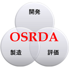
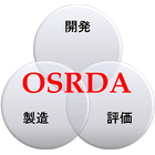
受託開発 受託開発
受託製造 受託製造
受託評価 受託評価
受託開発

受託開発

弊社は一般的なOSATやEMSのような製造受託や生産のみの請負ではなく、 研究開発にフォーカスし実装技術の開発受託を中心に対応しております。 お客様の研究開発部門の一つの機能として、実装技術の開発のアウトソーシング先としてご利用いただけます。 弊社の優位性としては、“委託自由度”、“幅広い接合技術”、“受託実績と未来性”、“高い協業力” がございます。

Revolutionizing Semiconductor Packaging! Connectec Japan's Challenge

Revitalizing Japan's manufacturing industry with the power to change and the power to connect.

We would like to introduce our philosophy of connecting companies, technology, and people to pave the way for the future of IoT implementation. Based in the semiconductor "back-end" hub that spans from the Joetsu region of Niigata Prefecture to Nagano Prefecture, we aim to create the world's first and best technologies. With our low-temperature packaging technology "MONSTER PAC" and fine wiring technology "FSNIP" as our weapons, we respond to various packaging needs. Together with like-minded colleagues, our mission is to contribute to society through job creation. *For more details on Connectec Japan's corporate philosophy and business overview, you can download it here.

Added to bookmarks

Bookmarks list

Bookmark has been removed

Bookmarks list

You can't add any more bookmarks

By registering as a member, you can increase the number of bookmarks you can save and organize them with labels.

Free membership registration

The explosive proliferation of IoT devices and the challenges of next-generation semiconductor implementation.

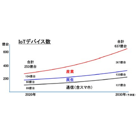
By 2030, it will reach 64 billion units. The evolution of hardware supporting the accelerating digital society.

With the advancement of IoT, new challenges of "heat" and "precision" are being presented in semiconductor packaging. The number of IoT devices, which was about 25 billion in 2020, is expected to reach approximately 64 billion by 2030. Many of these devices are composed of chips and substrates that are sensitive to heat, making it difficult to address them with conventional high-temperature packaging. To realize the virtual world with physical hardware, innovative technologies that operate at low temperatures and low thermal stress are essential. *Data summarizing the market forecasts and packaging challenges for IoT can be obtained here.*

Added to bookmarks

Bookmarks list

Bookmark has been removed

Bookmarks list

You can't add any more bookmarks

By registering as a member, you can increase the number of bookmarks you can save and organize them with labels.

Free membership registration

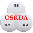
A new standard for outsourcing semiconductor packaging development called "OSRDA."

Flexible contract development that solves customers' "troubles."

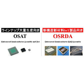
We provide total support for special projects that are impossible on existing mass production lines, from the conceptual stage to mass production. OSRDA (Outsourced Semiconductor R&D Assembly) is a business model that distinguishes itself from mere assembly specialists (OSAT). We can handle any process related to implementation, from substrate design, process development, and prototyping to reliability testing, at any stage and from any point. We offer flexible solutions tailored to our customers' preferences, such as multi-variety variable production and the development of special applications. *Please take a look at the materials that explain the specific service flow of OSRDA.

Added to bookmarks

Bookmarks list

Bookmark has been removed

Bookmarks list

You can't add any more bookmarks

By registering as a member, you can increase the number of bookmarks you can save and organize them with labels.

Free membership registration

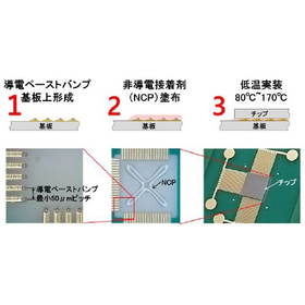
"MONSTER PAC" semiconductor packaging technology that achieves low temperature and high precision.

Low-temperature bonding from 80℃ unlocks the potential of heat-sensitive devices.

We have achieved high-precision mounting on thermally fragile chips and film substrates, which was impossible with conventional solder mounting. Standard solder joints require high temperatures of 260°C, but MONSTER PAC enables low-temperature bonding at 80°C to 170°C using conductive paste. This suppresses thermal expansion of materials and allows for narrow pitches of less than 40μm and high-precision mounting of less than 3μm. It is a suitable method for mounting advanced devices sensitive to heat, such as magnetic sensors and MEMS. *You can download the technical details and specifications of MONSTER PAC from here.*

Added to bookmarks

Bookmarks list

Bookmark has been removed

Bookmarks list

You can't add any more bookmarks

By registering as a member, you can increase the number of bookmarks you can save and organize them with labels.

Free membership registration

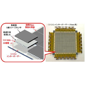
[Case 1] Realization of high sensitivity using 3D implemented chiplet X-ray sensors.

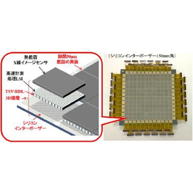
Successfully achieved 3D stacking of heat-sensitive sensors and semiconductor LSIs at low temperatures with ultra-high-density implementation at 50µm intervals.

How to integrate heat-sensitive image sensors with high-speed processing LSI. We solved this challenge with our unique 3D stacking technology. By 3D stacking heat-sensitive X-ray image sensors and TSV-forming LSI at low temperatures, we achieved direct bonding of the sensor pixel signal terminals. By arranging 144 sensors, each measuring 10mm on a side, with a minimal gap of 50µm, we enable large-area and high-sensitivity sensing. This is a case that condenses our know-how in utilizing silicon interposers to maximize high-speed measurement processing. *For specific processes of advanced 3D stacking technology, please refer to the materials.

Added to bookmarks

Bookmarks list

Bookmark has been removed

Bookmarks list

You can't add any more bookmarks

By registering as a member, you can increase the number of bookmarks you can save and organize them with labels.

Free membership registration

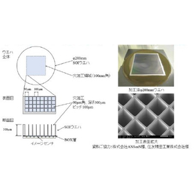
[Case 2] Micromachining Technology for Backside Illuminated X-ray Image Sensors

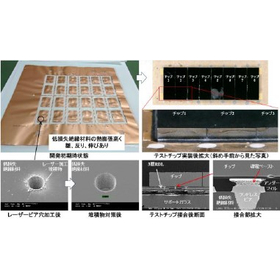
Maximizing the opening rate with 1 million corner hole formations. Challenging the limits of semiconductor wafer processing.

The realization of high-sensitivity sensors requires extremely precise wafer processing technology to expand the light-receiving area. We conducted a special processing to form 1 million square holes with a 100µm pitch on a Φ200mm photodiode wafer. By maintaining square holes of 90µm and a thin wall structure of 10µm, we achieved an overwhelming large aperture ratio and successfully enhanced sensitivity. This is a fine processing solution unique to Connectec Japan, utilizing deep dry etching (DRIE) on silicon wafers. *The accuracy of wafer processing and detailed specifications are available in the downloadable materials.

Added to bookmarks

Bookmarks list

Bookmark has been removed

Bookmarks list

You can't add any more bookmarks

By registering as a member, you can increase the number of bookmarks you can save and organize them with labels.

Free membership registration

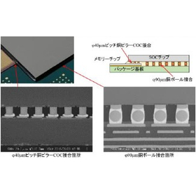
[Case 3] Shortest connection implementation solution for SOC + memory module

Overcoming the height difference between semiconductor chips! Innovative COC bonding with copper ball spacers.

We directly bonded memory chips and SOCs (COC) and responded to the advanced requirements of flip chip mounting onto package substrates. By coordinating the networks of four companies and ten processes, we successfully achieved bonding between heterogeneous chips of varying heights. Utilizing 40µm pitch copper pillar bonding and 90µm copper balls as spacers, we realized the shortest connections between chips and substrates. This structure, which maximizes signal transmission efficiency, provides a significant advantage in high-speed processing devices. *Details of the network that successfully integrates heterogeneous chips are illustrated in the accompanying materials.*

Added to bookmarks

Bookmarks list

Bookmark has been removed

Bookmarks list

You can't add any more bookmarks

By registering as a member, you can increase the number of bookmarks you can save and organize them with labels.

Free membership registration

Example 4: Advanced technology for millimeter-wave compatible three-layer RDL substrates and chip bonding.

Semiconductor implementation technology that achieves a 70GHz bandwidth. Completion of a complex 24-step process through collaboration among 15 companies.

We have developed a three-layer coplanar RDL substrate using low-loss insulating materials and simultaneously achieved high-precision bonding of millimeter-wave chips. We overcame technical challenges such as wrinkles and warping due to thermal expansion, as well as deposits during via processing, through thorough process improvements. By utilizing landless vias and three-layer impedance matching RDL, we ensured transmission characteristics over a wide bandwidth of 70 GHz. This is a top-tier example of realizing customer desires by managing 24 complex processes through the amoeba-like collaboration of 15 partner companies. *For detailed information on the millimeter-wave compatible implementation process and verification results, please refer to the downloadable materials.*

Added to bookmarks

Bookmarks list

Bookmark has been removed

Bookmarks list

You can't add any more bookmarks

By registering as a member, you can increase the number of bookmarks you can save and organize them with labels.

Free membership registration

Breaking through the challenges of the semiconductor industry! The CADN amoeba consortium starting with small-scale prototypes.

Backed by the collaboration of 300 domestic companies, we can achieve 'prototyping from a few pieces,' which is impossible for major OSATs.

In the early stages of development, a necessary "few to several dozen" prototypes. It is difficult for large companies to respond to this need, which is where our value lies. In large-scale companies like major foundries and OSATs that require significant investment recovery, mismatches in supply and demand for small-scale development projects tend to occur. "CADN" has established a decentralized production division model with small investments by organically connecting domestic legacy lines and research institutions. While hedging against regional risks such as earthquakes and floods, we have set up a system that can flexibly respond to a wide variety of structural and construction method requests. *For more details on the new business model "CADN," which consolidates Japan's manufacturing capabilities, please download here.

Added to bookmarks

Bookmarks list

Bookmark has been removed

Bookmarks list

You can't add any more bookmarks

By registering as a member, you can increase the number of bookmarks you can save and organize them with labels.

Free membership registration
Prev 1 Next
  • 金属・化学・窯業 食品・医薬品などの ほぐし・解砕 ふるい分けがこれ一台 解砕機構付き佐藤式振動ふるい機 つばさ デモ実施中!
  • 排気熱風なく 気温-4.1℃の冷風を 工事不要で暑さ対策 店舗・工場の 安全対策に! 気化式スポットクーラー Pure Drive ピュアドライブ
    • Contact this company

      Inquiry Form
    • Before making an inquiry

      Download Profile

    Products

    • Search for Products

    Company

    • Search for Companies

    Special Features

    • Special Features

    Ranking

    • Overall Products Ranking
    • Overall Company Ranking

    support

    • site map
    IPROS
    • privacy policy Regarding external transmission of information
    • terms of service
    • About Us
    • Careers
    • Advertising
    COPYRIGHT © 2001-2026 IPROS CORPORATION ALL RIGHTS RESERVED.
    Please note that the English text on this page is automatically translated and may contain inaccuracies.