- Publication year : 2026
1~5 item / All 5 items
Displayed results

Added to bookmarks
Bookmarks listBookmark has been removed
Bookmarks listYou can't add any more bookmarks
By registering as a member, you can increase the number of bookmarks you can save and organize them with labels.
Free membership registration
Contact this company
Inquiry Form1~5 item / All 5 items
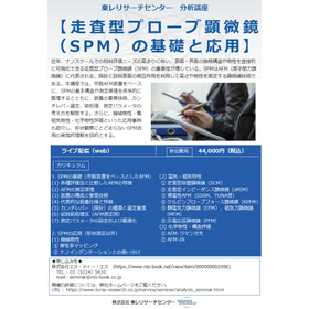
In recent years, with the increasing demand for material evaluation at the nanoscale, the importance of scanning probe microscopy (SPM), which can directly visualize the fine structures and physical properties of surfaces and interfaces, has grown. SPM is a microscopy technique represented by atomic force microscopy (AFM), which measures height and physical properties by utilizing the interaction between a probe and the sample surface. This course will systematically organize the basic structure and measurement principles of SPM based on commercially available AFM equipment, as well as explain the key technologies of the device, cantilever selection, sample preparation, and considerations for measurement parameters. Furthermore, application examples such as mechanical properties, electromagnetic properties, and chemical property evaluations will be introduced, aiming for a practical understanding of SPM utilization that goes beyond mere shape observation.
Added to bookmarks
Bookmarks listBookmark has been removed
Bookmarks listYou can't add any more bookmarks
By registering as a member, you can increase the number of bookmarks you can save and organize them with labels.
Free membership registration
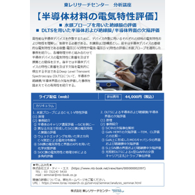
To create high-performance semiconductor devices, it is necessary to understand and control the electrical properties and physical characteristics of each material used in device fabrication. This course is structured in two parts: the first half introduces examples of applying mercury probe techniques to evaluate the basic electrical characteristics of semiconductor devices, such as capacitance-voltage (C-V) characteristics and current-voltage (I-V) characteristics, and demonstrates the relationship between the electrical properties of semiconductor devices and film quality in combination with various physical analyses. The second half presents Deep Level Transient Spectroscopy (DLTS), a method for electrically detecting defects that affect the characteristics of semiconductor devices, highlighting its usefulness based on examples of evaluating defects at semiconductor and insulating film/semiconductor interfaces.
Added to bookmarks
Bookmarks listBookmark has been removed
Bookmarks listYou can't add any more bookmarks
By registering as a member, you can increase the number of bookmarks you can save and organize them with labels.
Free membership registration
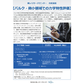
【Evaluation of the Mechanical Properties of Bulk Materials (Material Testing)】 The evaluation of the mechanical properties of materials aids in obtaining physical property values for design and simulation, as well as in elucidating material degradation phenomena. However, if accurate physical property values cannot be obtained, erroneous results may be derived. This course will explain the measurement methods for the mechanical properties of solid materials (static material tests such as tensile, bending, and compression) and introduce various measurement examples, along with the digital image correlation method that has been utilized in the field of mechanical property evaluation in recent years. 【Evaluation of Mechanical Properties in Microscopic Regions (Nanoindentation)】 The nanoindentation method is a technique that improves the load and displacement resolution of conventional hardness tests and is widely used for evaluating the mechanical properties of thin films and specific fine areas. In recent years, advancements in technology have enabled nanoindentation measurements that utilize environmental control functions and AFM capabilities. This course will introduce the basic principles and measurement modes, along with examples of each measurement.
Added to bookmarks
Bookmarks listBookmark has been removed
Bookmarks listYou can't add any more bookmarks
By registering as a member, you can increase the number of bookmarks you can save and organize them with labels.
Free membership registration
At the Toray Research Center, we offer analysis courses (paid seminars) conducted by experienced instructors. Starting in April 2026, we will launch new services for companies that request analysis, including the "Premium Annual Pass" and the "Premium 10 Sheet Pass." The Premium Pass is designed for multiple courses and multiple participants, targeting the analysis courses scheduled for the 2026 fiscal year (a total of 20 courses).
Added to bookmarks
Bookmarks listBookmark has been removed
Bookmarks listYou can't add any more bookmarks
By registering as a member, you can increase the number of bookmarks you can save and organize them with labels.
Free membership registration
On June 19, 2026 (Friday), Toray Research Center, Inc. will hold the "Semiconductor and Electronic Materials Poster Session 2026" at the Ota City Industrial Plaza (PiO) Large Hall in Tokyo, Kanto region. This event is primarily aimed at semiconductor device, equipment, and material manufacturers, and will introduce the latest analytical technologies and application examples in the semiconductor and electronic materials field through direct dialogue with researchers. On the day of the event, we plan to have: - 65 poster presentations covering the semiconductor and electronic materials field - Technical lectures focused on advanced devices, packaging, and material evaluation - Free discussions where participants can consult and discuss directly with researchers at the poster presentations ★ Pre-registration (free of charge) is required to participate in this event. On-the-day participation will not be allowed, so please be sure to register in advance via the link on the "Details & Registration" button below. ★ There is no participation fee. We sincerely look forward to your participation. 【Note】 We kindly ask representatives from competing companies to refrain from participating. Thank you for your understanding.
Added to bookmarks
Bookmarks listBookmark has been removed
Bookmarks listYou can't add any more bookmarks
By registering as a member, you can increase the number of bookmarks you can save and organize them with labels.
Free membership registration