

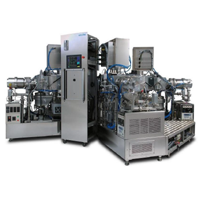
A high-precision sputtering device that contributes to wiring formation.
In the semiconductor industry, as miniaturization and high integration progress, the formation of reliable wiring is a crucial factor that influences product performance. In particular, the uniform deposition of wiring materials and stability in the process are essential for improving yield and extending product lifespan. Improper deposition can lead to a decline in electrical characteristics and potential early failures. Japan Create's sputtering equipment addresses these challenges and achieves high-quality wiring formation. 【Application Scenarios】 - Formation of wiring layers in semiconductor devices - Deposition of various metal thin films - Research and development applications 【Benefits of Implementation】 - Improved device performance through high-precision wiring formation - Yield enhancement through stable deposition processes - Flexibility to meet diverse needs
Inquire About This Product
basic information
【Features】 - Equipped with our unique spatter cathode - Achieves substrate temperature of 900°C with rapid heating mechanism - Enables high-speed and stable reactive sputtering deposition - Supports low-temperature processes such as lift-off - Compatible with tray transport 【Our Strengths】 Japan Create has pursued high precision, labor-saving, and miniaturization to meet the diverse needs of the semiconductor industry, continuously challenging cutting-edge technology. We seek infinite possibilities in high technology and create reliable know-how and uniqueness that match our customers' needs. As a manufacturer primarily of semiconductor production equipment, including wafer cleaning machines, etching devices, and spin dryers, we manufacture according to our customers' needs, from small research machines to fully automated mass production systems. At our Nagareyama facility's plasma process equipment division, a team of engineers specialized in vacuum and plasma technology responds to a wide variety of customer needs. Since all products are manufactured in-house, we can offer them at competitive prices.
Price range
Delivery Time
Applications/Examples of results
【Custom Manufacturing Achievements (Excerpt)】 ■ Ultra-high temperature sputtering equipment for thin film MEMS ■ Batch-type multi-target sputtering equipment ■ Batch-type sputtering equipment for thin film MEMS ■ IBS equipment for research and development ■ Composite film deposition equipment for MEMS ■ Multi-target composite sputtering equipment ■ Sputtering equipment with GB for organic EL, etc. *For more details, please refer to the PDF document or feel free to contact us.
catalog(1)
Download All Catalogs
Company information

Japan Create has been challenging cutting-edge technologies to respond to the diversification of the semiconductor industry with high precision, labor-saving, and miniaturization. We seek infinite possibilities in high technology and create reliable know-how that matches user needs with our uniqueness. We will continue to strive towards high-level technology.


