
List of Sputtering Equipment products
- classification:Sputtering Equipment
1~45 item / All 209 items


Reduce the workload from handling heavy objects! Here are five case studies that solved customer challenges! We are also accepting free consultations and tests tailored to your work!

- Other conveying machines


We can accommodate high resistance over 10,000 ohms, with diameters ranging from approximately 30 mm to 8 inches, and we also offer thinning and chip processing arrangements!
- Other semiconductors
- Processing Contract
- Wafer


Composite thin film experimental device nanoPVD-ST15A capable of mixed installation of vacuum deposition (metal and organic deposition sources) and sputtering cathodes.
- Sputtering Equipment
- Evaporation Equipment

■□【PyroMini】□■ Compact High-Performance Infrared Temperature Sensor
High-performance touch panel converter for easy setup, data logging, and data storage on microSD card. The PM2.2 model can also measure glossy metal surfaces. 【Overview】 With a highly visible high-brightness touch panel display, parameters such as temperature range, emissivity, and sampling rate can be intuitively operated and set. Long-term data storage and management are possible with a microSD card. (*An option for a converter without a display is also available.) The compact sensor head, measuring φ18mm x 45mm, allows for temperature measurement in tight spaces. It employs sensors and cables with excellent noise resistance, making it suitable for integration into moving equipment such as robotic arms. The PM2.2 model uses a short wavelength of 2.2um, supporting high temperatures (Max 2000℃) and measurements of glossy metal material surfaces. 【Features】 ◎ Wide range: -20 to 1000℃ (PM), 100 to 2000℃ (PM2.2) ◎ Excellent basic performance: Accuracy ±1%, reproducibility ±0.5%, 240msec fast response ◎ Measurement wavelength range: 8 to 14μm (PM), 2.0 to 2.2μm (PM2.2) ◎ Compact Φ18mm x 45mm
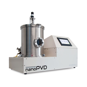
Sputter Cathode and Co-evaporation Source Mixed Thin Film Experimental Device: Metal deposition, organic deposition, and sputter cathode installed in a compact frame.
- Sputtering Equipment
- Evaporation Equipment
- Annealing furnace
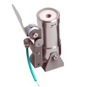
◆OLED◆ Organic vapor deposition - High-temperature metal evaporation source Max 1500℃
The OLED evaporation source is a high-temperature heating heater for vacuum devices with a maximum operating temperature of 1500°C. It can evaporate materials with high evaporation temperatures, making it suitable for a wide range of applications as a vacuum high-temperature heater and evaporation cell, from low-temperature organic deposition (up to 800°C) cells to high-temperature resistance heating deposition (up to 1500°C) MBE cells. Shutter actuators and water-cooled jackets are also available. High-temperature heaters above 800°C are designed with internal shielding, considering insulation and thermal shielding. 【Main Specifications】 ■ Maximum control temperature: 800°C or 1500°C ■ Operating environment: in vacuum or inert gas (*O2 up to 800°C) ■ Heater: tungsten filament ■ Crucible volume: 1cc (maximum fill volume 1.5cc) ■ Crucible material: alumina ■ Case material: SUS304 or molybdenum ■ Thermocouple: K or C 【Options】 ⚫ Crucible material: PBN, graphite, quartz ⚫ Heater: NiCr wire, Kanthal wire (*for O2) ⚫ Crucible volume: 10cc (maximum fill volume 15cc) ⚫ Shutter: pneumatic or motor-driven ⚫ Water-cooled jacket ⚫ Controller (for heater and shutter control)

Two thin-film experimental devices are connected with a load-lock mechanism. Different film deposition devices (sputtering, evaporation, etc.) are seamlessly connected with the load-lock.
- Sputtering Equipment
- Evaporation Equipment
- Etching Equipment

[SH Vacuum Substrate Additional High-Temperature Plate Heater_Max 1100℃] For CVD and PVD Vacuum Thin Films
ThermoCera Japan has updated the latest catalog for its ultra-high temperature substrate heating heaters, suitable for thin film experiments such as CVD and PVD, ranging from 1 inch to 4 inches. ◉ Maximum operating temperature: 850°C (SH-IN), 1100°C (SH-BN) We also accommodate requests for customized products such as substrate holders, vertical lift mechanisms, substrate rotation mechanisms, and RF bias. Additionally, we offer heater controllers in both traditional standalone models and 19-inch rack mount options.

High-performance multi-sputtering device 6-element multi-sputter (for Φ4 inch) 4-element multi-sputter (for Φ6, 8 inch)
- Sputtering Equipment
- Evaporation Equipment
- Etching Equipment

【MiniLab】 Evaporation/Sputtering Dual Chamber System
Two thin film experimental devices are connected by a load lock mechanism. Different film deposition devices (sputtering - evaporation, etc.) are seamlessly connected via the load lock. With Moorfield's unique load lock system, connections to the process chamber on the left, right, and rear are also possible (see photo below). 1. MiniLab-E080A (Evaporation Device) - EB evaporation: 7cc crucible x 6 - Resistance heating evaporation x 2 - Organic evaporation limit x 2 2. MiniLab-S060A (Sputtering Device) - Φ2" Magnetron cathode x 4 for simultaneous sputtering - Compatible with both DC and RF power supplies 3. Load Lock Chamber - Plasma etching stage In the load lock chamber, plasma cleaning of the substrate surface is performed using the "RF/DC substrate bias stage," and the company's unique "soft etching" technology allows for a <30W low-power, damage-free plasma etching stage. This enables delicate etching processes that are prone to damage, such as 2D (removal of resists like PMMA), graphene delamination, and etching of Teflon substrates. (*This can also be installed in the main chamber stage.)

A semi-custom-made thin film experimental device that can be assembled with the desired configuration for processes such as sputtering, EB (electron beam), and annealing.
- Evaporation Equipment
- Sputtering Equipment
- Annealing furnace
【MiniLab】 Evaporation/Sputtering Dual Chamber System
Two thin film experimental devices are connected by a load lock mechanism. Different film deposition devices (sputtering - evaporation, etc.) are seamlessly connected via the load lock. With Moorfield's unique load lock system, connections to the process chamber on the left, right, and rear are also possible (see photo below). 1. MiniLab-E080A (Evaporation Device) - EB evaporation: 7cc crucible x 6 - Resistance heating evaporation x 2 - Organic evaporation limit x 2 2. MiniLab-S060A (Sputtering Device) - Φ2" Magnetron cathode x 4 for simultaneous sputtering - Compatible with both DC and RF power supplies 3. Load Lock Chamber - Plasma etching stage In the load lock chamber, plasma cleaning of the substrate surface is performed using the "RF/DC substrate bias stage," and the company's unique "soft etching" technology allows for a <30W low-power, damage-free plasma etching stage. This enables delicate etching processes that are prone to damage, such as 2D (removal of resists like PMMA), graphene delamination, and etching of Teflon substrates. (*This can also be installed in the main chamber stage.)

Two thin film experimental devices are connected with a load lock mechanism. Different film deposition devices (sputtering, evaporation, etc.) are seamlessly connected with the load lock.
- Sputtering Equipment
- Evaporation Equipment
- Etching Equipment
【MiniLab】 Evaporation/Sputtering Dual Chamber System
Two thin film experimental devices are connected by a load lock mechanism. Different film deposition devices (sputtering - evaporation, etc.) are seamlessly connected via the load lock. With Moorfield's unique load lock system, connections to the process chamber on the left, right, and rear are also possible (see photo below). 1. MiniLab-E080A (Evaporation Device) - EB evaporation: 7cc crucible x 6 - Resistance heating evaporation x 2 - Organic evaporation limit x 2 2. MiniLab-S060A (Sputtering Device) - Φ2" Magnetron cathode x 4 for simultaneous sputtering - Compatible with both DC and RF power supplies 3. Load Lock Chamber - Plasma etching stage In the load lock chamber, plasma cleaning of the substrate surface is performed using the "RF/DC substrate bias stage," and the company's unique "soft etching" technology allows for a <30W low-power, damage-free plasma etching stage. This enables delicate etching processes that are prone to damage, such as 2D (removal of resists like PMMA), graphene delamination, and etching of Teflon substrates. (*This can also be installed in the main chamber stage.)

High-performance multi-sputtering device 6-element multi-sputter (for Φ4 inch) 4-element multi-sputter (for Φ6, 8 inch)
- Sputtering Equipment
- Evaporation Equipment
- Etching Equipment
◆OLED◆ Organic vapor deposition - High-temperature metal evaporation source Max 1500℃
The OLED evaporation source is a high-temperature heating heater for vacuum devices with a maximum operating temperature of 1500°C. It can evaporate materials with high evaporation temperatures, making it suitable for a wide range of applications as a vacuum high-temperature heater and evaporation cell, from low-temperature organic deposition (up to 800°C) cells to high-temperature resistance heating deposition (up to 1500°C) MBE cells. Shutter actuators and water-cooled jackets are also available. High-temperature heaters above 800°C are designed with internal shielding, considering insulation and thermal shielding. 【Main Specifications】 ■ Maximum control temperature: 800°C or 1500°C ■ Operating environment: in vacuum or inert gas (*O2 up to 800°C) ■ Heater: tungsten filament ■ Crucible volume: 1cc (maximum fill volume 1.5cc) ■ Crucible material: alumina ■ Case material: SUS304 or molybdenum ■ Thermocouple: K or C 【Options】 ⚫ Crucible material: PBN, graphite, quartz ⚫ Heater: NiCr wire, Kanthal wire (*for O2) ⚫ Crucible volume: 10cc (maximum fill volume 15cc) ⚫ Shutter: pneumatic or motor-driven ⚫ Water-cooled jacket ⚫ Controller (for heater and shutter control)

High-performance, cost-effective RF/DC magnetron sputtering device for research and development.
- Other semiconductor manufacturing equipment
- Sputtering Equipment

4-Yen Multi-Sputtering Device 【MiniLab-S060】
4 cathodes with Φ2 inch configuration Simultaneous film deposition: 3-component simultaneous deposition (RF 500W or DC 850W) + HiPIMS (PulseDC 5KW) x 1 Power distribution and configuration settings for 4 cathodes can be freely changed via the HMI screen using the plasma relay switch 3 MFC systems (Ar, O2, N2) for reactive sputtering RIE etching stage RF 300W (main chamber) + <30W soft etching (LL chamber) Substrate heating: Max 500℃, 800℃, or 1000℃ (C/C or SiC coating) Substrate rotation and vertical movement (automatically controlled by stepping motor) APC automatic control: Upstream (MFC flow adjustment) or downstream (automatic valve opening adjustment on the exhaust side) Dimensions: 1,120(W) x 800(D) ● Mixed specifications for resistance heating deposition, organic material deposition, EB deposition, PECVD, etc. are also possible.
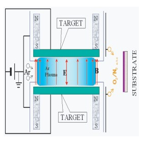

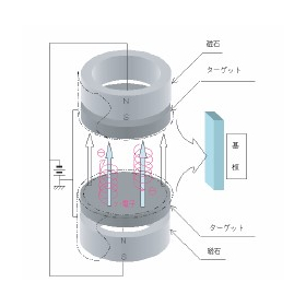
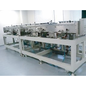
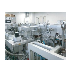
No damage to the substrate! A vacuum deposition device capable of ultra-low temperature sputtering.
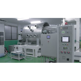
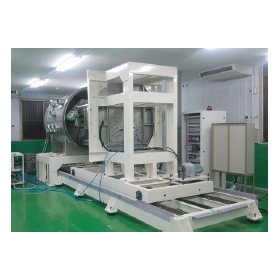
- Sputtering Equipment
![[Hot Stage] Ultra High Temperature ...](https://image.mono.ipros.com/public/product/image/671/2000002653/IPROS21404174246949592221.png?w=280&h=280)
An ultra-high temperature substrate heating stage that allows for substrate elevation, rotation, and RF/DC substrate bias all in one device! 'All-In-One' component.
- Sputtering Equipment
■□【PyroMini】□■ Compact High-Performance Infrared Temperature Sensor
High-performance touch panel converter for easy setup, data logging, and data storage on microSD card. The PM2.2 model can also measure glossy metal surfaces. 【Overview】 With a highly visible high-brightness touch panel display, parameters such as temperature range, emissivity, and sampling rate can be intuitively operated and set. Long-term data storage and management are possible with a microSD card. (*An option for a converter without a display is also available.) The compact sensor head, measuring φ18mm x 45mm, allows for temperature measurement in tight spaces. It employs sensors and cables with excellent noise resistance, making it suitable for integration into moving equipment such as robotic arms. The PM2.2 model uses a short wavelength of 2.2um, supporting high temperatures (Max 2000℃) and measurements of glossy metal material surfaces. 【Features】 ◎ Wide range: -20 to 1000℃ (PM), 100 to 2000℃ (PM2.2) ◎ Excellent basic performance: Accuracy ±1%, reproducibility ±0.5%, 240msec fast response ◎ Measurement wavelength range: 8 to 14μm (PM), 2.0 to 2.2μm (PM2.2) ◎ Compact Φ18mm x 45mm

A compact multi-thin film device that incorporates sputtering, deposition, electron beam (EB), and annealing thin film modules in a 60-liter volume chamber, suitable for various applications.
- Sputtering Equipment
- Evaporation Equipment
- CVD Equipment
【MiniLab】 Evaporation/Sputtering Dual Chamber System
Two thin film experimental devices are connected by a load lock mechanism. Different film deposition devices (sputtering - evaporation, etc.) are seamlessly connected via the load lock. With Moorfield's unique load lock system, connections to the process chamber on the left, right, and rear are also possible (see photo below). 1. MiniLab-E080A (Evaporation Device) - EB evaporation: 7cc crucible x 6 - Resistance heating evaporation x 2 - Organic evaporation limit x 2 2. MiniLab-S060A (Sputtering Device) - Φ2" Magnetron cathode x 4 for simultaneous sputtering - Compatible with both DC and RF power supplies 3. Load Lock Chamber - Plasma etching stage In the load lock chamber, plasma cleaning of the substrate surface is performed using the "RF/DC substrate bias stage," and the company's unique "soft etching" technology allows for a <30W low-power, damage-free plasma etching stage. This enables delicate etching processes that are prone to damage, such as 2D (removal of resists like PMMA), graphene delamination, and etching of Teflon substrates. (*This can also be installed in the main chamber stage.)

Flexible configuration available upon request for methods such as deposition, sputtering, and EB. Adopts a tall chamber with a height of 570mm, contributing to improved uniformity during deposition.
- Evaporation Equipment
- Sputtering Equipment
- Etching Equipment
【MiniLab】 Evaporation/Sputtering Dual Chamber System
Two thin film experimental devices are connected by a load lock mechanism. Different film deposition devices (sputtering - evaporation, etc.) are seamlessly connected via the load lock. With Moorfield's unique load lock system, connections to the process chamber on the left, right, and rear are also possible (see photo below). 1. MiniLab-E080A (Evaporation Device) - EB evaporation: 7cc crucible x 6 - Resistance heating evaporation x 2 - Organic evaporation limit x 2 2. MiniLab-S060A (Sputtering Device) - Φ2" Magnetron cathode x 4 for simultaneous sputtering - Compatible with both DC and RF power supplies 3. Load Lock Chamber - Plasma etching stage In the load lock chamber, plasma cleaning of the substrate surface is performed using the "RF/DC substrate bias stage," and the company's unique "soft etching" technology allows for a <30W low-power, damage-free plasma etching stage. This enables delicate etching processes that are prone to damage, such as 2D (removal of resists like PMMA), graphene delamination, and etching of Teflon substrates. (*This can also be installed in the main chamber stage.)

Compact and space-saving! Ideal for research and development, flexible configuration for purposes such as deposition, sputtering, and annealing.
- Evaporation Equipment
- Sputtering Equipment
- Annealing furnace
【MiniLab】 Evaporation/Sputtering Dual Chamber System
Two thin film experimental devices are connected by a load lock mechanism. Different film deposition devices (sputtering - evaporation, etc.) are seamlessly connected via the load lock. With Moorfield's unique load lock system, connections to the process chamber on the left, right, and rear are also possible (see photo below). 1. MiniLab-E080A (Evaporation Device) - EB evaporation: 7cc crucible x 6 - Resistance heating evaporation x 2 - Organic evaporation limit x 2 2. MiniLab-S060A (Sputtering Device) - Φ2" Magnetron cathode x 4 for simultaneous sputtering - Compatible with both DC and RF power supplies 3. Load Lock Chamber - Plasma etching stage In the load lock chamber, plasma cleaning of the substrate surface is performed using the "RF/DC substrate bias stage," and the company's unique "soft etching" technology allows for a <30W low-power, damage-free plasma etching stage. This enables delicate etching processes that are prone to damage, such as 2D (removal of resists like PMMA), graphene delamination, and etching of Teflon substrates. (*This can also be installed in the main chamber stage.)

Due to its modular embedded design, it is possible to flexibly assemble dedicated equipment according to the required film formation method. A compact thin-film experimental device that can accommodat...
- Sputtering Equipment
■□【PyroMini】□■ Compact High-Performance Infrared Temperature Sensor
High-performance touch panel converter for easy setup, data logging, and data storage on microSD card. The PM2.2 model can also measure glossy metal surfaces. 【Overview】 With a highly visible high-brightness touch panel display, parameters such as temperature range, emissivity, and sampling rate can be intuitively operated and set. Long-term data storage and management are possible with a microSD card. (*An option for a converter without a display is also available.) The compact sensor head, measuring φ18mm x 45mm, allows for temperature measurement in tight spaces. It employs sensors and cables with excellent noise resistance, making it suitable for integration into moving equipment such as robotic arms. The PM2.2 model uses a short wavelength of 2.2um, supporting high temperatures (Max 2000℃) and measurements of glossy metal material surfaces. 【Features】 ◎ Wide range: -20 to 1000℃ (PM), 100 to 2000℃ (PM2.2) ◎ Excellent basic performance: Accuracy ±1%, reproducibility ±0.5%, 240msec fast response ◎ Measurement wavelength range: 8 to 14μm (PM), 2.0 to 2.2μm (PM2.2) ◎ Compact Φ18mm x 45mm

Compact and space-saving! Ideal for research and development. Flexible configuration for purposes such as deposition, sputtering, and annealing.
- Evaporation Equipment
- Sputtering Equipment
- Annealing furnace
■□【PyroMini】□■ Compact High-Performance Infrared Temperature Sensor
High-performance touch panel converter for easy setup, data logging, and data storage on microSD card. The PM2.2 model can also measure glossy metal surfaces. 【Overview】 With a highly visible high-brightness touch panel display, parameters such as temperature range, emissivity, and sampling rate can be intuitively operated and set. Long-term data storage and management are possible with a microSD card. (*An option for a converter without a display is also available.) The compact sensor head, measuring φ18mm x 45mm, allows for temperature measurement in tight spaces. It employs sensors and cables with excellent noise resistance, making it suitable for integration into moving equipment such as robotic arms. The PM2.2 model uses a short wavelength of 2.2um, supporting high temperatures (Max 2000℃) and measurements of glossy metal material surfaces. 【Features】 ◎ Wide range: -20 to 1000℃ (PM), 100 to 2000℃ (PM2.2) ◎ Excellent basic performance: Accuracy ±1%, reproducibility ±0.5%, 240msec fast response ◎ Measurement wavelength range: 8 to 14μm (PM), 2.0 to 2.2μm (PM2.2) ◎ Compact Φ18mm x 45mm

High-efficiency magnetron sputtering cathode compatible with RF, DC, and pulse DC for depositing metals and insulators without impurities. It also excels in maintainability.
- Sputtering Equipment
■□【PyroMini】□■ Compact High-Performance Infrared Temperature Sensor
High-performance touch panel converter for easy setup, data logging, and data storage on microSD card. The PM2.2 model can also measure glossy metal surfaces. 【Overview】 With a highly visible high-brightness touch panel display, parameters such as temperature range, emissivity, and sampling rate can be intuitively operated and set. Long-term data storage and management are possible with a microSD card. (*An option for a converter without a display is also available.) The compact sensor head, measuring φ18mm x 45mm, allows for temperature measurement in tight spaces. It employs sensors and cables with excellent noise resistance, making it suitable for integration into moving equipment such as robotic arms. The PM2.2 model uses a short wavelength of 2.2um, supporting high temperatures (Max 2000℃) and measurements of glossy metal material surfaces. 【Features】 ◎ Wide range: -20 to 1000℃ (PM), 100 to 2000℃ (PM2.2) ◎ Excellent basic performance: Accuracy ±1%, reproducibility ±0.5%, 240msec fast response ◎ Measurement wavelength range: 8 to 14μm (PM), 2.0 to 2.2μm (PM2.2) ◎ Compact Φ18mm x 45mm
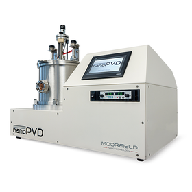
High-performance, cost-effective RF/DC magnetron sputtering system for research and development.
- Sputtering Equipment
- Evaporation Equipment
- Other semiconductor manufacturing equipment
■□【PyroMini】□■ Compact High-Performance Infrared Temperature Sensor
High-performance touch panel converter for easy setup, data logging, and data storage on microSD card. The PM2.2 model can also measure glossy metal surfaces. 【Overview】 With a highly visible high-brightness touch panel display, parameters such as temperature range, emissivity, and sampling rate can be intuitively operated and set. Long-term data storage and management are possible with a microSD card. (*An option for a converter without a display is also available.) The compact sensor head, measuring φ18mm x 45mm, allows for temperature measurement in tight spaces. It employs sensors and cables with excellent noise resistance, making it suitable for integration into moving equipment such as robotic arms. The PM2.2 model uses a short wavelength of 2.2um, supporting high temperatures (Max 2000℃) and measurements of glossy metal material surfaces. 【Features】 ◎ Wide range: -20 to 1000℃ (PM), 100 to 2000℃ (PM2.2) ◎ Excellent basic performance: Accuracy ±1%, reproducibility ±0.5%, 240msec fast response ◎ Measurement wavelength range: 8 to 14μm (PM), 2.0 to 2.2μm (PM2.2) ◎ Compact Φ18mm x 45mm

Compact and space-saving! Ideal for research and development. Flexible configuration for purposes such as deposition, sputtering, and annealing.
- Evaporation Equipment
- Sputtering Equipment
- Etching Equipment
【MiniLab】 Evaporation/Sputtering Dual Chamber System
Two thin film experimental devices are connected by a load lock mechanism. Different film deposition devices (sputtering - evaporation, etc.) are seamlessly connected via the load lock. With Moorfield's unique load lock system, connections to the process chamber on the left, right, and rear are also possible (see photo below). 1. MiniLab-E080A (Evaporation Device) - EB evaporation: 7cc crucible x 6 - Resistance heating evaporation x 2 - Organic evaporation limit x 2 2. MiniLab-S060A (Sputtering Device) - Φ2" Magnetron cathode x 4 for simultaneous sputtering - Compatible with both DC and RF power supplies 3. Load Lock Chamber - Plasma etching stage In the load lock chamber, plasma cleaning of the substrate surface is performed using the "RF/DC substrate bias stage," and the company's unique "soft etching" technology allows for a <30W low-power, damage-free plasma etching stage. This enables delicate etching processes that are prone to damage, such as 2D (removal of resists like PMMA), graphene delamination, and etching of Teflon substrates. (*This can also be installed in the main chamber stage.)

Storage-compatible glove box PVD flexible thin film experimental device, featuring a tall chamber with a height of 570mm, contributes to improved uniformity during deposition.
- Evaporation Equipment
- Sputtering Equipment
- Annealing furnace
【MiniLab】 Evaporation/Sputtering Dual Chamber System
Two thin film experimental devices are connected by a load lock mechanism. Different film deposition devices (sputtering - evaporation, etc.) are seamlessly connected via the load lock. With Moorfield's unique load lock system, connections to the process chamber on the left, right, and rear are also possible (see photo below). 1. MiniLab-E080A (Evaporation Device) - EB evaporation: 7cc crucible x 6 - Resistance heating evaporation x 2 - Organic evaporation limit x 2 2. MiniLab-S060A (Sputtering Device) - Φ2" Magnetron cathode x 4 for simultaneous sputtering - Compatible with both DC and RF power supplies 3. Load Lock Chamber - Plasma etching stage In the load lock chamber, plasma cleaning of the substrate surface is performed using the "RF/DC substrate bias stage," and the company's unique "soft etching" technology allows for a <30W low-power, damage-free plasma etching stage. This enables delicate etching processes that are prone to damage, such as 2D (removal of resists like PMMA), graphene delamination, and etching of Teflon substrates. (*This can also be installed in the main chamber stage.)

Due to its modular embedded design, it is possible to flexibly assemble dedicated equipment according to the required film deposition method. A compact thin-film experimental device that can accommoda...
- Sputtering Equipment
- Evaporation Equipment
- Etching Equipment
【MiniLab】 Evaporation/Sputtering Dual Chamber System
Two thin film experimental devices are connected by a load lock mechanism. Different film deposition devices (sputtering - evaporation, etc.) are seamlessly connected via the load lock. With Moorfield's unique load lock system, connections to the process chamber on the left, right, and rear are also possible (see photo below). 1. MiniLab-E080A (Evaporation Device) - EB evaporation: 7cc crucible x 6 - Resistance heating evaporation x 2 - Organic evaporation limit x 2 2. MiniLab-S060A (Sputtering Device) - Φ2" Magnetron cathode x 4 for simultaneous sputtering - Compatible with both DC and RF power supplies 3. Load Lock Chamber - Plasma etching stage In the load lock chamber, plasma cleaning of the substrate surface is performed using the "RF/DC substrate bias stage," and the company's unique "soft etching" technology allows for a <30W low-power, damage-free plasma etching stage. This enables delicate etching processes that are prone to damage, such as 2D (removal of resists like PMMA), graphene delamination, and etching of Teflon substrates. (*This can also be installed in the main chamber stage.)

Due to its modular embedded design, it is possible to flexibly assemble dedicated machines according to the required film formation methods. A compact thin-film experimental device that can accommodat...
- Sputtering Equipment
- Evaporation Equipment
- Annealing furnace
【MiniLab】 Evaporation/Sputtering Dual Chamber System
Two thin film experimental devices are connected by a load lock mechanism. Different film deposition devices (sputtering - evaporation, etc.) are seamlessly connected via the load lock. With Moorfield's unique load lock system, connections to the process chamber on the left, right, and rear are also possible (see photo below). 1. MiniLab-E080A (Evaporation Device) - EB evaporation: 7cc crucible x 6 - Resistance heating evaporation x 2 - Organic evaporation limit x 2 2. MiniLab-S060A (Sputtering Device) - Φ2" Magnetron cathode x 4 for simultaneous sputtering - Compatible with both DC and RF power supplies 3. Load Lock Chamber - Plasma etching stage In the load lock chamber, plasma cleaning of the substrate surface is performed using the "RF/DC substrate bias stage," and the company's unique "soft etching" technology allows for a <30W low-power, damage-free plasma etching stage. This enables delicate etching processes that are prone to damage, such as 2D (removal of resists like PMMA), graphene delamination, and etching of Teflon substrates. (*This can also be installed in the main chamber stage.)

A semi-custom-made thin film experimental device that can be assembled with the desired configuration for processes such as evaporation, sputtering, electron beam (EB) deposition, and annealing.
- Evaporation Equipment
- Sputtering Equipment
- Etching Equipment
■□【PyroMini】□■ Compact High-Performance Infrared Temperature Sensor
High-performance touch panel converter for easy setup, data logging, and data storage on microSD card. The PM2.2 model can also measure glossy metal surfaces. 【Overview】 With a highly visible high-brightness touch panel display, parameters such as temperature range, emissivity, and sampling rate can be intuitively operated and set. Long-term data storage and management are possible with a microSD card. (*An option for a converter without a display is also available.) The compact sensor head, measuring φ18mm x 45mm, allows for temperature measurement in tight spaces. It employs sensors and cables with excellent noise resistance, making it suitable for integration into moving equipment such as robotic arms. The PM2.2 model uses a short wavelength of 2.2um, supporting high temperatures (Max 2000℃) and measurements of glossy metal material surfaces. 【Features】 ◎ Wide range: -20 to 1000℃ (PM), 100 to 2000℃ (PM2.2) ◎ Excellent basic performance: Accuracy ±1%, reproducibility ±0.5%, 240msec fast response ◎ Measurement wavelength range: 8 to 14μm (PM), 2.0 to 2.2μm (PM2.2) ◎ Compact Φ18mm x 45mm

Compact multi-film device that incorporates sputtering, deposition, EB, and annealing thin film modules in a 60L volume chamber, suitable for various applications.
- Sputtering Equipment
- Evaporation Equipment
- CVD Equipment
【MiniLab】 Evaporation/Sputtering Dual Chamber System
Two thin film experimental devices are connected by a load lock mechanism. Different film deposition devices (sputtering - evaporation, etc.) are seamlessly connected via the load lock. With Moorfield's unique load lock system, connections to the process chamber on the left, right, and rear are also possible (see photo below). 1. MiniLab-E080A (Evaporation Device) - EB evaporation: 7cc crucible x 6 - Resistance heating evaporation x 2 - Organic evaporation limit x 2 2. MiniLab-S060A (Sputtering Device) - Φ2" Magnetron cathode x 4 for simultaneous sputtering - Compatible with both DC and RF power supplies 3. Load Lock Chamber - Plasma etching stage In the load lock chamber, plasma cleaning of the substrate surface is performed using the "RF/DC substrate bias stage," and the company's unique "soft etching" technology allows for a <30W low-power, damage-free plasma etching stage. This enables delicate etching processes that are prone to damage, such as 2D (removal of resists like PMMA), graphene delamination, and etching of Teflon substrates. (*This can also be installed in the main chamber stage.)

Storage-compatible glove box PVD flexible thin film experimental device, featuring a tall chamber with a height of 570mm, contributes to improved uniformity during deposition.
- Evaporation Equipment
- Sputtering Equipment
- Etching Equipment
■□【PyroMini】□■ Compact High-Performance Infrared Temperature Sensor
High-performance touch panel converter for easy setup, data logging, and data storage on microSD card. The PM2.2 model can also measure glossy metal surfaces. 【Overview】 With a highly visible high-brightness touch panel display, parameters such as temperature range, emissivity, and sampling rate can be intuitively operated and set. Long-term data storage and management are possible with a microSD card. (*An option for a converter without a display is also available.) The compact sensor head, measuring φ18mm x 45mm, allows for temperature measurement in tight spaces. It employs sensors and cables with excellent noise resistance, making it suitable for integration into moving equipment such as robotic arms. The PM2.2 model uses a short wavelength of 2.2um, supporting high temperatures (Max 2000℃) and measurements of glossy metal material surfaces. 【Features】 ◎ Wide range: -20 to 1000℃ (PM), 100 to 2000℃ (PM2.2) ◎ Excellent basic performance: Accuracy ±1%, reproducibility ±0.5%, 240msec fast response ◎ Measurement wavelength range: 8 to 14μm (PM), 2.0 to 2.2μm (PM2.2) ◎ Compact Φ18mm x 45mm


Packaging and packing machines, as well as vacuum pumps! We offer a full range of equipment from the main units to components in various fields.
- Other measurement, recording and measuring instruments
- Sputtering Equipment
- Used goods purchase

Introduction of various experimental devices for research and development in semiconductors, electronic devices, fuel cells, displays, and thin film experiments.
- Sputtering Equipment
- Evaporation Equipment
- Annealing furnace
■□【PyroMini】□■ Compact High-Performance Infrared Temperature Sensor
High-performance touch panel converter for easy setup, data logging, and data storage on microSD card. The PM2.2 model can also measure glossy metal surfaces. 【Overview】 With a highly visible high-brightness touch panel display, parameters such as temperature range, emissivity, and sampling rate can be intuitively operated and set. Long-term data storage and management are possible with a microSD card. (*An option for a converter without a display is also available.) The compact sensor head, measuring φ18mm x 45mm, allows for temperature measurement in tight spaces. It employs sensors and cables with excellent noise resistance, making it suitable for integration into moving equipment such as robotic arms. The PM2.2 model uses a short wavelength of 2.2um, supporting high temperatures (Max 2000℃) and measurements of glossy metal material surfaces. 【Features】 ◎ Wide range: -20 to 1000℃ (PM), 100 to 2000℃ (PM2.2) ◎ Excellent basic performance: Accuracy ±1%, reproducibility ±0.5%, 240msec fast response ◎ Measurement wavelength range: 8 to 14μm (PM), 2.0 to 2.2μm (PM2.2) ◎ Compact Φ18mm x 45mm
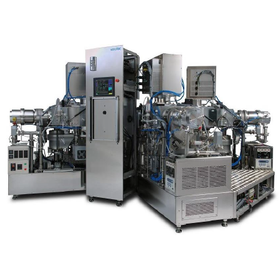

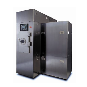
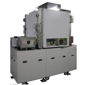
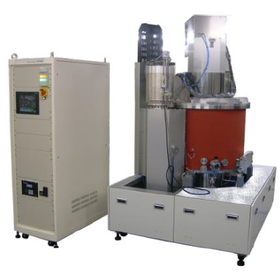
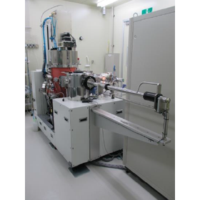
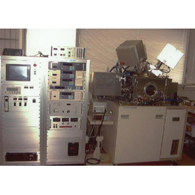
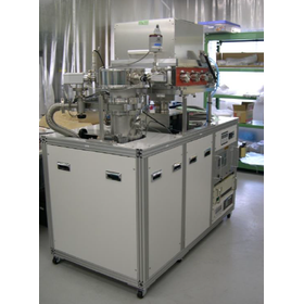
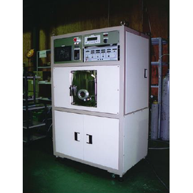
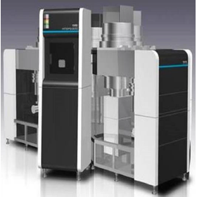
A high-precision sputtering device that contributes to wiring formation.
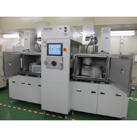
- Sputtering Equipment


Metal films and protective films can be deposited automatically on resin substrates!
- Vacuum Equipment
- Sputtering Equipment
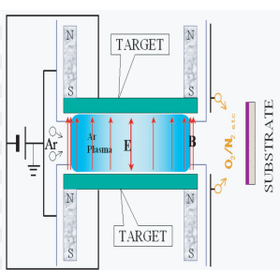
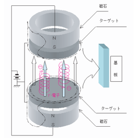
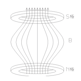
Large area sputtering is possible! Film deposition can be achieved even without cooling.
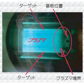
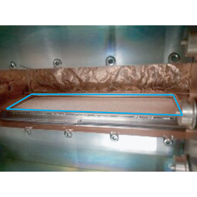
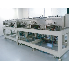
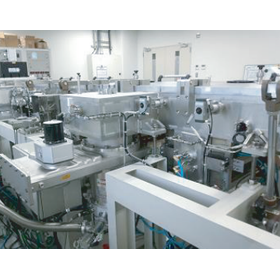
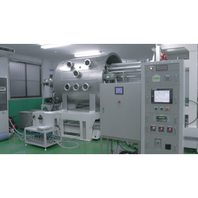
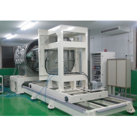
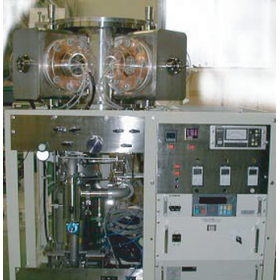
- Sputtering Equipment


Expansion to advanced packages: Processing is possible on a 510×515mm substrate.
- Sputtering Equipment
- Etching Equipment
- Annealing furnace


The "FHR.Star.600-EOSS" is a high-performance magnetron sputtering device developed for precise optical filter film deposition.


- Sputtering Equipment

Highly acclaimed high-precision optical filter deposition magnetron sputtering device
This is a device specialized in optical thin films, such as high-performance optical filters that require multilayering and high reproducibility, particularly for applications like LiDAR, which are expected to see significant demand in the future. It demonstrates strong capabilities for high-quality and stable production. - Film formation that eliminates the influence of film quality changes due to target consumption using a cylindrical cathode. - Stable film formation of oxide films achieved by incorporating a reactive ion source. - Film formation of a wide range of multilayer films enabled by the installation of up to four cathodes.

A high ion current helicon plasma ion source PVD module that achieves directional film formation and enables reactive sputtering.


- Sputtering Equipment
- Plasma Generator

High-throughput roll-to-roll sputtering equipment for the manufacture of FCCL (Flexible Copper Clad Laminate).
- Sputtering Equipment

FHR Star.100-Tetra Co is a very compact sputtering device designed for MEMS and high-performance optical products.
- Sputtering Equipment

High-performance, high-quality magnetron sputtering cathodes! Sales, repair, and maintenance services are also available.
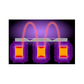

- Sputtering Equipment
- Vacuum Equipment
- Other metal materials

The Spatakaso Sword Service Center has been established.
Starting in April 2024, we will establish a service center for inspection and repair of the "Magnetron Sputter Cathode" manufactured by Angstrome Science in the United States. The new service center will be equipped with clean room facilities, vacuum leak checkers, and various inspection instruments to ensure comprehensive maintenance. All work will be supervised and guided by qualified personnel who have completed training at Angstrome Science, providing services similar to those in the United States. Until now, we have primarily focused on repairs due to malfunctions, but with the opening of the service center, we will also be able to offer regular maintenance. We will conduct periodic inspections of the cathodes to support operations without downtime.

High-rate and high-quality film formation of dielectric and ferromagnetic materials.


- Sputtering Equipment

We will exhibit at the MEMS Engineer Forum 2025.
The MEMS Engineer Forum is a unique forum operated primarily by engineers among the key players in MEMS technology, which is considered a key technology of the 21st century. At this forum, where MEMS researchers, developers, and engineers from around the world gather, we will introduce and showcase the Remote Plasma Ion Beam Sputtering System manufactured by Plasma Quest Ltd. This is an excellent opportunity to see cutting-edge technologies related to MEMS, not only from our exhibition but also from others. We cordially invite you to attend. Venue: International Fashion Center Hall 1-6-1 Yokogawa, Sumida-ku, Tokyo 130-0015, Japan Access: https://www.tokyo-kfc.co.jp/access/ Exhibited Product: Remote Plasma Ion Beam Sputtering System by Plasma Quest Ltd. https://mono.ipros.com/product/detail/2001148974 https://www.plasmaquest.com/

Production ion beam milling equipment that achieves high rate and high reliability.

- Sputtering Equipment

We achieve film formation by freely controlling reactive sputtering and alloy sputtering.


- Sputtering Equipment
- Plasma Generator
- Other surface treatment equipment

We have updated the page for the remote plasma ion beam sputtering system manufactured by PlasmaQuest.
We have updated the page for the Remote Plasma Ion Beam Sputtering System manufactured by PlasmaQuest, which has received positive feedback from various companies since its introduction. We have also included a video on Remote Plasma Target Bias Sputtering. If you have any questions or requests, please feel free to contact us.

Remote source ion beam sputtering device manufacturer for remote plasma sources.

- Sputtering Equipment

Information on commissioned test film formation services (test film formation of high-quality reaction films, etc.)
Research on Co-sputtering of different materials, such as ferromagnetic targets and metal and ceramic targets, which are considered difficult to film using conventional sputtering devices. We strongly support advanced material research and process development, including the deposition of AlScN, which is attracting attention for next-generation MEMS applications. This is a groundbreaking technology that uses a helicon ion source as a plasma source, accelerating high-density ions obtained from it by applying a bias voltage to the target. Since it is an ion beam-type deposition method using a remote plasma system, stable film formation can be achieved even with ferromagnetic and dielectric targets, which are challenging for magnetron sputtering devices. By individually controlling the ion source and target application, it is possible to accommodate a wide range of deposition conditions while also achieving high deposition rates. Independent gas supply near the target and substrate allows for the deposition of various multilayer thin films, including oxide and nitride films. Since the substrate surface is not exposed to plasma, it is possible to maintain a low temperature during film formation.

We will extend the life of your equipment with bolt-on and coupler-on solutions.


- Sputtering Equipment
- Solenoid Actuators
- Transport and handling robots

Developed for the purpose of achieving high uniformity and excellent reproducibility in the deposition of optical multilayer films!
- Sputtering Equipment

Optimal solution for high-rate reactive film deposition production equipment.


- Sputtering Equipment