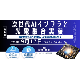
9/17 Webinar "Next-Generation AI Infrastructure and Optoelectronic Fusion Implementation"

Responding to the rapidly increasing amount of information in AI and video! An explanation from the basics of high-speed information transmission to optoelectronic integration implementation, semiconductor and optical transmission technologies, and future challenges!
■Title: "Next-Generation AI Infrastructure and Optoelectronic Integration Implementation - Addressing Massive Information Processing and Decoding Optoelectronic Integration -" ――In the context of the rapid increase in information volume due to AI and live video, this seminar explains optical fiber communication, high-speed wireless, and semiconductor technologies that support high-speed information transmission. Participants will systematically learn about the current status and challenges of "optoelectronic integration implementation" aimed at introducing optical transmission between and within electronic devices. 【Knowledge Gained from the Seminar】 - Basics of high-speed information transmission technology and the essence of high-speed transmission - Factors influencing high-speed transmission such as transmission medium, transmission distance, and transmission loss - Transmission methods including wired/wireless, 4G/5G, Wi-Fi 6/7 - Development history of optical fiber communication, communication methods, and transceivers - Challenges in information transmission between and within electronic devices - Status of research on optoelectronic signal conversion and optoelectronic integration implementation - Basic technologies such as optical semiconductors, silicon photonics, processors, and memory 【Target Audience for the Seminar】 - Individuals interested in high-speed information transmission technology - Those dealing with large-capacity information such as AI and video - Individuals who want to learn the fundamentals of semiconductors and transmission technology
Inquire About This Product
basic information
■Event Details Date and Time: September 17, 2026 (Thursday) 10:30 AM - 4:30 PM Participation Fee: 55,000 yen (tax included) *Includes materials *Newsletter subscribers: 49,500 yen (tax included) Method of Attendance: This seminar will be a live-streamed seminar using "Zoom." Instructor: Shigeru Koshibe CEO of iPack Specialization: Development of base materials in the semiconductor and optical fields, semiconductor packaging materials, optical materials, and optoelectronic integration-related technologies.
Price information
Participation Fee: 55,000 yen (tax included) *Includes materials *For our newsletter members (registration is free) 49,500 yen (tax included) ★【Newsletter Member Benefit】If two or more people apply at the same time and all applicants register as newsletter members, the participation fee per person will be half of the newsletter member price.
Delivery Time
Applications/Examples of results
For details about the program and how to apply, please check the related link URL.
Company information

We provide the latest industrial insights to our clients. By conducting market trend analysis, publishing technology‑related books and research reports, and organizing and managing seminars, we support research and development across a wide range of industries, with a primary focus on manufacturing. Our coverage spans diverse fields such as energy, batteries, chemicals, and biotechnology.