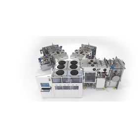
Fully automatic deposition device equipped with up to 4 chambers, achieving high throughput with cassette-to-cassette operation.
Multi BAK is a fully automated deposition device that integrates up to four BAK process chambers around a central atmospheric transport handler. By eliminating manual labor through cassette-to-cassette processing and utilizing innovative handling and load-lock technology, it achieves reduced processing time, improved process reproducibility, and reduced energy consumption of the device. It enhances throughput for mass production applications and lowers the cost of ownership (CoO). *For more details, please feel free to contact us.*

Inquire About This Product
basic information
【Configuration】 ■ Integration of up to 4 BAK process chambers around a central atmospheric transport handler ■ Fully automated cassette-to-cassette processing ■ Reduced processing time through load lock technology * For detailed specifications, board sizes, and throughput, please contact us.
Price range
Delivery Time
Applications/Examples of results
Main Uses of BAK Family ■ Power Devices: Backside metallization with high material utilization efficiency, lift-off process ■ Wireless: IDT electrodes for TF-SAW ■ Precision Optics: Optical thin films from UV to IR ■ MEMS: Film deposition of metals, dielectrics, and TCO, co-evaporation process
Company information
Evatec's technology has been utilized worldwide for 70 years since the establishment of Balzers AG in 1946. Now, Evatec's thin film manufacturing technology is revolutionizing our lives and ways of working. The Internet of Things (IoT) offers the potential to connect 7 trillion devices for a global population of 7 billion people, and Evatec's thin film manufacturing technology makes this possible. Semiconductor devices manufactured with Evatec's equipment enable millions of people around the world to connect through high-speed wireless networks, changing the way we work due to the evolution of AI. Additionally, autonomous driving made possible by AI semiconductors and high-precision sensing is transforming lifestyles, while power semiconductors allow various devices to operate with less power, addressing energy issues. We provide cutting-edge solutions for thin film manufacturing with high-performance electrical and optical properties, ranging from high-frequency filters essential for wireless communication, high-brightness LEDs for automotive and lighting applications, AI and optoelectronic integrated semiconductors for highly integrated data centers, to touch panels for mobile phones.