World Semiconductor Process Control System Industry Report 2026: Market Size Projected to Grow to 20,259 Million USD
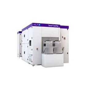
A semiconductor process control system refers to a comprehensive set of inspection and measurement devices and related software that performs defect inspection, dimension measurement, film thickness measurement, pattern alignment, surface shape analysis, and more during the manufacturing process of semiconductor wafers and photomasks. Utilizing technologies such as optics, electron beams, X-rays, and scanning probes, it plays a role in detecting minute defects and process variations to prevent yield loss. The system includes wafer inspection and defect review devices, wafer measurement devices, mask inspection and defect review devices, and mask measurement devices.
Inquire About This Product
basic information
Global Market Size of Semiconductor Process Control Systems According to the latest research report published by Global Reports titled "Global Market Size, Share, Company Rankings, Revenue, and Demand Trend Forecast for Semiconductor Process Control Systems (2026-2032)," the global market size for semiconductor process control systems is expected to expand from approximately 17 billion USD in 2025 to about 20.259 billion USD in 2026. The compound annual growth rate (CAGR) from 2026 to 2032 is projected to be 14.0%, reaching approximately 44.491 billion USD by 2032. The miniaturization and high stacking of advanced logic, DRAM, and 3D NAND, along with the proliferation of advanced packaging including HBM and chiplets, are major factors driving the demand for inspection and measurement in semiconductor process control systems.
Price range
Delivery Time
Applications/Examples of results
Wafer inspection and measurement systems form the core of semiconductor process control systems. Semiconductor process control systems can be broadly divided into four areas: wafer inspection systems, wafer measurement systems, mask inspection systems, and mask measurement systems, depending on the inspection target and measurement purpose. Wafer inspection systems detect foreign substances, defects, and pattern anomalies present on unpatterned wafers or wafers after circuit formation, while defect review systems identify the type and cause of defects using high-resolution images. On the other hand, wafer measurement systems quantitatively measure parameters such as circuit line width, overlay accuracy, film thickness, surface shape, and stress using tools like CD-SEM and optical measurement devices. The mask-related equipment in semiconductor process control systems is responsible for defect inspection, dimensional measurement, and pattern position accuracy evaluation of photomasks and EUV masks. Tiny defects on the mask can affect multiple chips through the transfer to the wafer, making mask blank inspection and patterned mask inspection highly important. Particularly in EUV lithography, there is a demand for addressing defects that are difficult to detect with conventional optical inspection, leading to the development of actinic inspection techniques utilizing 13.5nm EUV light and high-sensitivity electron beam inspection technologies.
Company information

Global Reports integrates industrial information from around the world and provides highly accurate market intelligence to support corporate decision-making. We deliver in-depth analyses based on numerical data and facts, including market size, share, industry structure, price trends, growth forecasts, rankings of major companies, and competitive trends, with clear information categorized by country, region, and application. Leveraging a rich database that has supported the business growth of over 65,000 companies and an international research network, we accompany our clients in their global expansion and continuous growth.