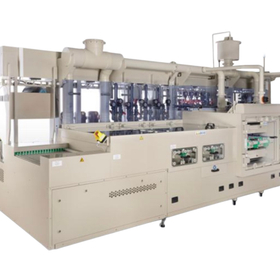
ICP etching equipment for compound semiconductor processes
The RIE-330iPC is a multi-wafer processing etching device for compound semiconductor processes that employs an inductively coupled plasma (ICP) discharge method. 【Features】 ○ Compatible with large trays of Φ330mm Up to 27 pieces for Φ2-inch wafers, 17 pieces for Φ2.5-inch wafers, 12 pieces for Φ3-inch wafers, 7 pieces for Φ4-inch wafers, and 3 pieces for Φ6-inch wafers can be processed simultaneously. ○ By adopting the new SSTC (Symmetrical Shielded Tornado Coil) electrode as the ICP source, it enables high selectivity and excellent uniformity in etching over large areas. ○ Allows for low-damage processes at low bias (below -100V). ○ Stable etching conditions can be achieved through temperature control of the substrate stage and the inner walls of the reaction chamber. ○ A turbo molecular pump is also used in the load lock chamber, providing a more stable process.

Inquire About This Product
basic information
The RIE-330iPC is a multi-wafer processing etching device for compound semiconductor processes that employs an inductively coupled plasma (ICP) discharge method. 【Features】 - Compatible with large trays of Φ330mm - Can process 27 pieces of Φ2-inch wafers, 17 pieces of Φ2.5-inch wafers, 12 pieces of Φ3-inch wafers, 7 pieces of Φ4-inch wafers, and 3 pieces of Φ6-inch wafers simultaneously. - By adopting the new SSTC (Symmetrical Shielded Tornado Coil) electrode as the ICP source, it enables high selectivity and excellent uniformity in etching over large areas. - Allows for low-damage processes at low bias (below -100V). - Stable etching conditions can be achieved through temperature control of the substrate stage and the inner walls of the reaction chamber. - A turbo molecular pump is also used in the load lock chamber to provide a more stable process.
Price information
-
Delivery Time
Applications/Examples of results
【Application Examples】 Fabrication of GaN-based electronic devices and light-emitting devices For more details, please request materials or download the catalog.
Company information

We excel in the technology of thin film formation and processing at the nano to micro level, and we are well-regarded for providing equipment and technology for both research and development applications as well as production purposes. Additionally, we specialize in the optoelectronics field, particularly in light sources (LEDs and semiconductor lasers), which are expected to see market expansion in the future.


![[Custom-made Specialized Equipment Manufacturing Case] Annealing Device](https://image.mono.ipros.com/public/product/image/c9b/2001133077/IPROS00457043333246552069.png?w=280&h=280)