
List of Semiconductor Manufacturing Equipment products
- classification:Semiconductor Manufacturing Equipment
301~315 item / All 5250 items


It won't break even after 1 million repetitions! A mat switch with reliable operation, high durability, and low price. Suitable for options in machine tools as well. Please consult us about delivery t...
- Sensors


We can accommodate high resistance over 10,000 ohms, with diameters ranging from approximately 30 mm to 8 inches, and we also offer thinning and chip processing arrangements!
- Other semiconductors
- Processing Contract
- Wafer


High-performance multi-sputtering device 6-element multi-sputter (for Φ4 inch) 4-element multi-sputter (for Φ6, 8 inch)
- Sputtering Equipment
- Evaporation Equipment
- Etching Equipment

The catalog for the MiniLab Flexible Thin Film Experimental Device has been renewed!
We have completely renewed the catalog for the MiniLab series thin film experimental equipment. 【Features of the MiniLab Series】 ◉ Supports sputtering, evaporation (resistive heating, organic, EB), annealing, plasma etching, etc. ◉ Modular design allows for flexible combinations of components (source hybrid types and multi-chamber configurations are possible) ◉ Compact, space-saving design (width 1,200 x depth 560 mm) ◉ Excellent operability: intuitive interface allows for centralized management of all operations via a touch panel without dispersion. We are confident that this will be of great assistance in research and development settings. Please consider it.

We have incorporated all the latest vacuum deposition technology into a compact benchtop-sized device that can effectively utilize limited lab space.
- Evaporation Equipment

◆nanoPVD-T15A◆ High-performance organic and metal film deposition device
Ideal for organic thin film deposition applications such as OLED, OPV, and OTFT. Utilizes low-temperature organic deposition sources with excellent temperature responsiveness/stability and high-temperature deposition sources for metal films. A fully automated R&D vacuum deposition system with easy touch panel operation, excellent operability, and maintainability. An intuitive HMI that allows anyone to operate without complicated procedures. Connects to a PC via USB cable for log saving and creating and storing automatic deposition recipes. ◉ Compact size: 804(W) x 530(D) x 600(H)mm ◉ Weight: 40kg to 70kg (depending on equipment configuration) ◉ Excellent basic performance - Achievable vacuum level: 5x10⁻⁵ Pascal - Equipped with a high-performance turbo molecular pump - Φ2 inch or Φ4 inch substrates ◉ Deposition sources - Resistance heating deposition source TE x up to 2 units - Organic deposition source LTE x up to 4 units (if mixed with resistance heating TE, up to 2 units) ◉ 7" touch panel ◉ Continuous deposition - Automatic control of deposition programs - 30 types of registered recipes - High-precision wide-range vacuum gauge ◉ Abundant options - Substrate rotation - Up and down lift with 300mm stroke - Substrate shutter - Dry pump (RP standard)

Introduction of various experimental devices for research and development in semiconductors, electronic devices, fuel cells, displays, and thin film experiments.
- Sputtering Equipment
- Evaporation Equipment
- Annealing furnace
◆nanoPVD-T15A◆ High-performance organic and metal film deposition device
Ideal for organic thin film deposition applications such as OLED, OPV, and OTFT. Utilizes low-temperature organic deposition sources with excellent temperature responsiveness/stability and high-temperature deposition sources for metal films. A fully automated R&D vacuum deposition system with easy touch panel operation, excellent operability, and maintainability. An intuitive HMI that allows anyone to operate without complicated procedures. Connects to a PC via USB cable for log saving and creating and storing automatic deposition recipes. ◉ Compact size: 804(W) x 530(D) x 600(H)mm ◉ Weight: 40kg to 70kg (depending on equipment configuration) ◉ Excellent basic performance - Achievable vacuum level: 5x10⁻⁵ Pascal - Equipped with a high-performance turbo molecular pump - Φ2 inch or Φ4 inch substrates ◉ Deposition sources - Resistance heating deposition source TE x up to 2 units - Organic deposition source LTE x up to 4 units (if mixed with resistance heating TE, up to 2 units) ◉ 7" touch panel ◉ Continuous deposition - Automatic control of deposition programs - 30 types of registered recipes - High-precision wide-range vacuum gauge ◉ Abundant options - Substrate rotation - Up and down lift with 300mm stroke - Substrate shutter - Dry pump (RP standard)


Waterproofing and miniaturization of physical AI electronic components! High reliability hot melt molding sealing for protecting automotive electronic components!
- Circuit board design and manufacturing
- Other polymer materials
- Molding Equipment
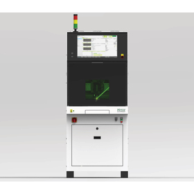

An innovative technology that heats the bond, making it easier to wedge bond copper wire.
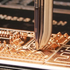
- Bonding Equipment

A controllable current transducer and frequency that continuously monitors wire deformation.
- Bonding Equipment

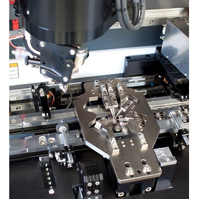
Expansion of productivity! The large work area allows for batch processing of multiple devices.
- Bonding Equipment

Dual-head wedge bonder for high-speed, high-precision, and high-productivity lead frames.
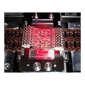
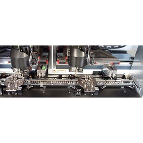
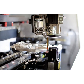
- Bonding Equipment
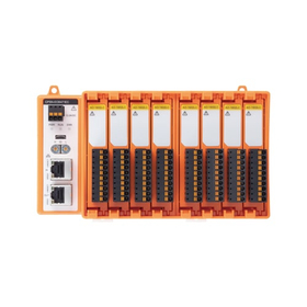

Modular remote I/O coupler unit that can efficiently configure the number of I/O points supported by EtherNet/IP.
- Other semiconductor manufacturing equipment
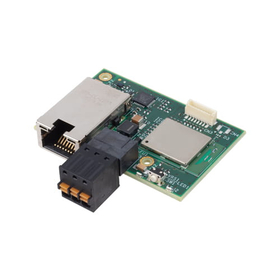
Modular remote I/O coupler unit that can efficiently configure the number of I/O points supported by EtherNet/IP.
- Other semiconductor manufacturing equipment