
List of Other semiconductor manufacturing equipment products
- classification:Other semiconductor manufacturing equipment
1~45 item / All 2042 items


Reduce the workload from handling heavy objects! Here are five case studies that solved customer challenges! We are also accepting free consultations and tests tailored to your work!

- Other conveying machines


We can accommodate high resistance over 10,000 ohms, with diameters ranging from approximately 30 mm to 8 inches, and we also offer thinning and chip processing arrangements!
- Other semiconductors
- Processing Contract
- Wafer


Safe even at 1000℃. An insulating material suitable for thermal design.
- Other machine elements
- Other processing machines
- Other semiconductor manufacturing equipment


Next-generation megasonic technology can instantly clear wafers up to 300mm.
- Photomask
- Other semiconductor manufacturing equipment
- Ultrasonic Cleaner

Announcement of the product page launch for the SONOSYS Megasonic Cleaning Nozzle System | Precision Cleaning for Semiconductors and MEMS
We are pleased to announce that Tick Corporation has launched a product introduction page for the SONOSYS megasonic cleaning nozzle system. The megasonic cleaning technology from SONOSYS utilizes high-frequency energy ranging from 600 kHz to 9 MHz to precisely remove fine particles while minimizing damage to microstructures such as semiconductor wafers, photomasks, and MEMS. The new page features the characteristics of single, double, and triple nozzles, as well as applications for semiconductors, MEMS, optical components, and LCD/FPD substrates. If you are considering fine particle removal, precision cleaning using ultra-pure water (DI Water), or megasonic cleaning at frequencies such as 600 kHz or 1 MHz, please take a look.
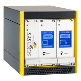
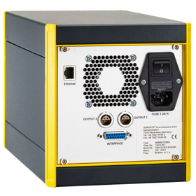
The Digital Generator is a digital control generator compatible with megasonic cleaning systems for semiconductors, electronic components, and precision instruments.
- Photomask
- Other semiconductor manufacturing equipment
- Wafer
Announcement of the product page launch for the SONOSYS Megasonic Cleaning Nozzle System | Precision Cleaning for Semiconductors and MEMS
We are pleased to announce that Tick Corporation has launched a product introduction page for the SONOSYS megasonic cleaning nozzle system. The megasonic cleaning technology from SONOSYS utilizes high-frequency energy ranging from 600 kHz to 9 MHz to precisely remove fine particles while minimizing damage to microstructures such as semiconductor wafers, photomasks, and MEMS. The new page features the characteristics of single, double, and triple nozzles, as well as applications for semiconductors, MEMS, optical components, and LCD/FPD substrates. If you are considering fine particle removal, precision cleaning using ultra-pure water (DI Water), or megasonic cleaning at frequencies such as 600 kHz or 1 MHz, please take a look.


It is a manufacturer specializing in filter housings.
- Other semiconductor manufacturing equipment
- Other filters
- Filtration Equipment

We are a manufacturer specializing in filter housings.
- Other semiconductor manufacturing equipment
- Other filters
- Filtration Equipment

We are a manufacturer specializing in filter housings.
- Other semiconductor manufacturing equipment
- Other filters
- Filtration Equipment

It is a manufacturer specializing in filter housings.
- Other semiconductor manufacturing equipment
- Beverage Production Equipment
- Filtration Equipment

We are a manufacturer specializing in filter housings.
- Other semiconductor manufacturing equipment
- Other filters
- Filtration Equipment

We are a manufacturer specializing in filter housings.
- Other semiconductor manufacturing equipment
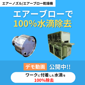

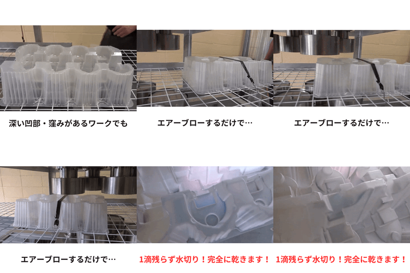
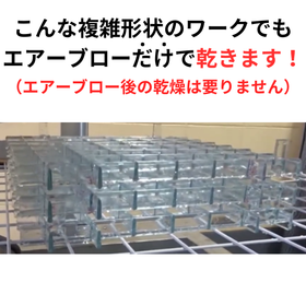
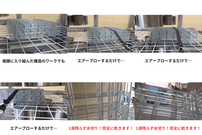
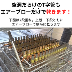
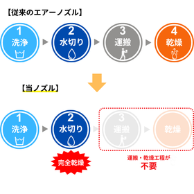
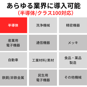
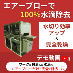
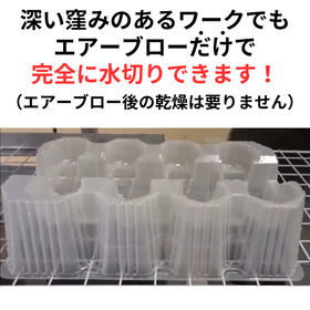
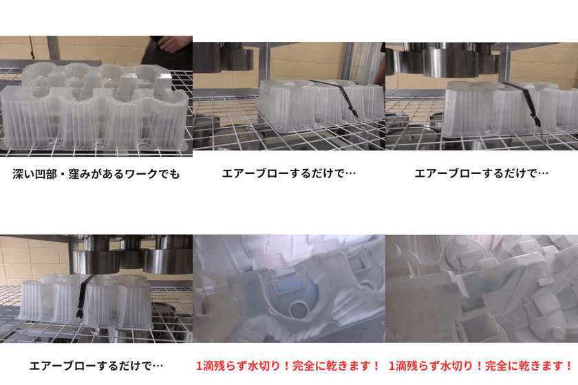
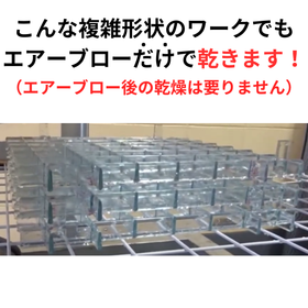
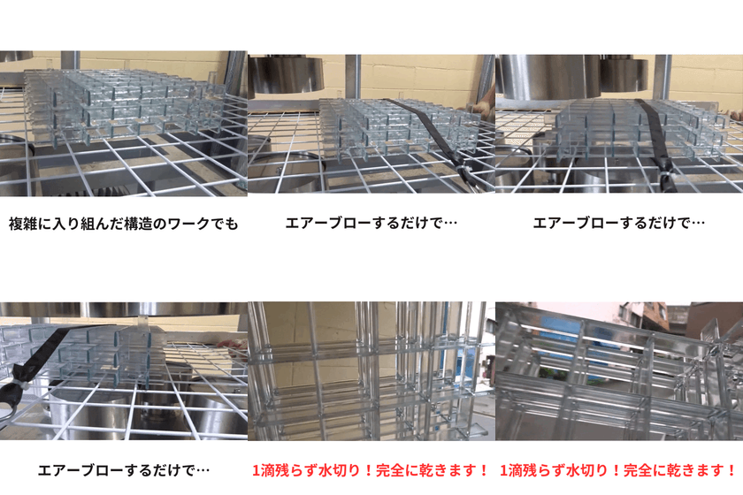
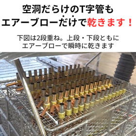
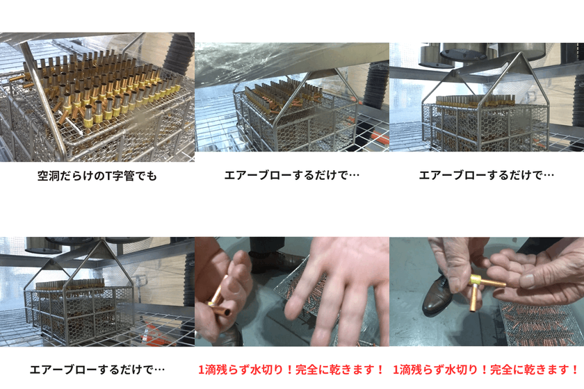
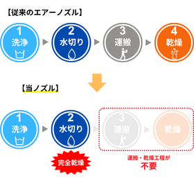
[Patent Obtained] Instant complete water removal of workpieces with air blow = complete drying!
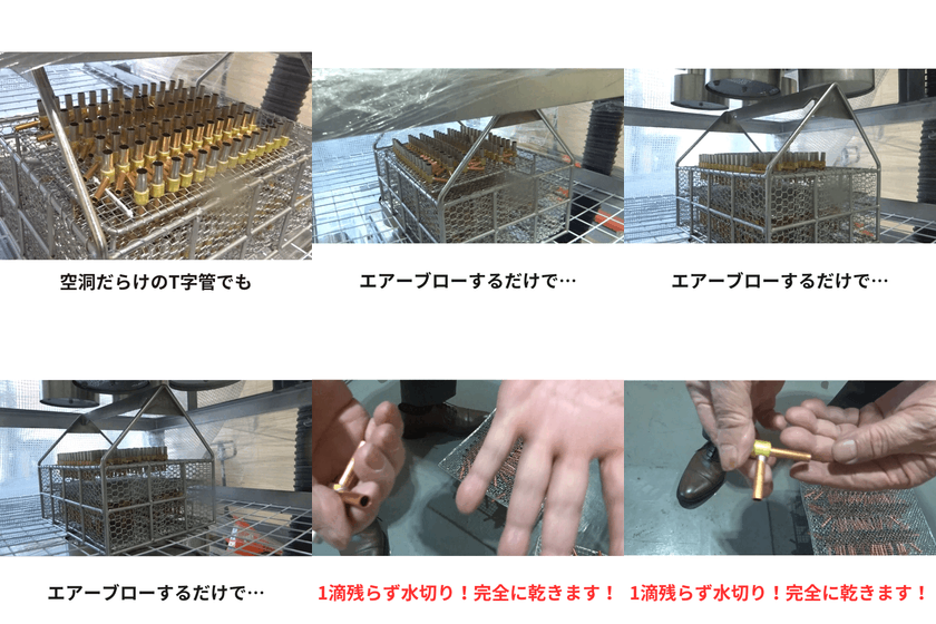
- Other semiconductor manufacturing equipment

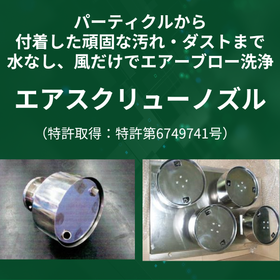
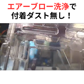
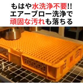
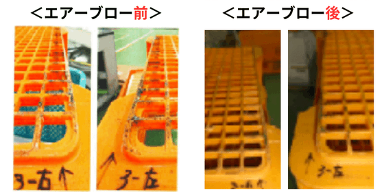
Revolutionary! No need for water washing! Particles are removed with just air blow.
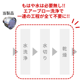
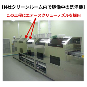
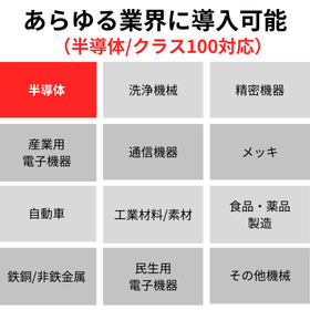
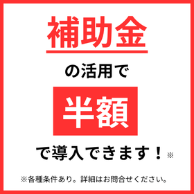
- Other semiconductor manufacturing equipment
Are you making this mistake when draining water from your work?
- Other semiconductor manufacturing equipment


Are you making this mistake with the work's drainage?


- Other semiconductor manufacturing equipment

Are you making this mistake while draining water from the work?
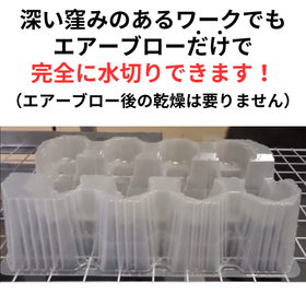
[To those in charge who are struggling with workpiece water drainage] Are you making these mistakes with workpiece water drainage? ✓ Do you know the real reason why, even if you increase the air blow pressure, not all water droplets are blown away? ✓ Do you know the real reason why, even if you increase the number of air nozzles, water is not sufficiently drained? ✓ Do you know the real reason why, even if you change the shape of the air nozzle, it still does not drain water effectively? These mistakes are typical errors made by companies that use air blow for workpiece water drainage and droplet removal. However, these mistakes are not significant compared to a certain "fatal mistake." What is that "fatal mistake"? It is… We provide this information in a PDF file. Download it now to find out.

No more revolution! No need for washing; particles are removed with just air blowing.


- Other semiconductor manufacturing equipment

Just by looking at this, you'll understand everything! We created a PR flyer (dust removal version).
Thoroughly remove dust from workpieces with air blow! We have summarized everything about the patented complete dust removal air nozzle, "Air Screw Nozzle," on a single A4 flyer. "What kind of nozzle is it?" "Why can it remove dust so effectively?" "How can it remove dust even from complex-shaped workpieces?" Just by looking at this, you can quickly understand everything about the Air Screw Nozzle. Please download and take a look.

[Patent Obtained] Complete water removal in an instant with air blow = complete drying!


- Other semiconductor manufacturing equipment

If you see this, you'll understand everything! I created a PR flyer.
100% water removal with air blow! No water droplets left on the workpiece! We have summarized everything about the patented complete drying air nozzle, "Air Screw Nozzle," on a single A4 flyer. "What kind of nozzle is it?" "Can it really remove 100% of the water?" "Why is it so effective at removing water?" Just by looking at this, you can quickly understand everything about the Air Screw Nozzle. Please download it and take a look!
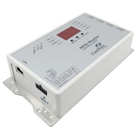

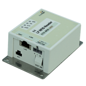
One unit supports 4 channels! Cost reduction and space-saving possible!
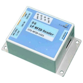
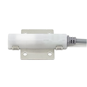
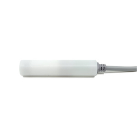
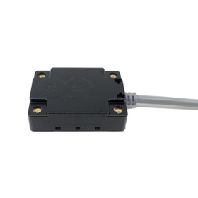
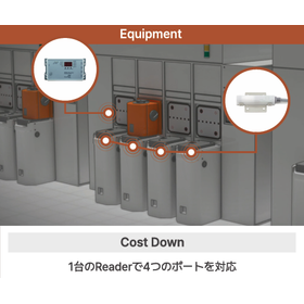
- Other semiconductor manufacturing equipment

HJS K-Series Bellows Pump for Semiconductor Manufacturing Equipment | High Quality, Low Pulsation, High Durability
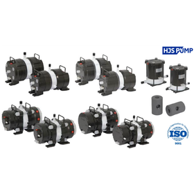
- Other semiconductor manufacturing equipment


Are you having trouble with the delivery time for cast prototypes? "Casting prototype service!" for cast iron, aluminum castings, and stainless steel castings (lost wax casting)!
- Other semiconductor manufacturing equipment




Automatically distill 1ppb grade hydrochloric acid, hydrofluoric acid, and nitric acid to 10ppt grade, reducing the procurement costs of high-purity acids.
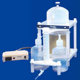
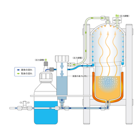
- Other semiconductor manufacturing equipment
- Distillation Apparatus

Achievements in the semiconductor industry worldwide, including the United States and Japan. A range of PFA products that contribute with outstanding reliability and purity.
- Other semiconductor manufacturing equipment


OptiSeal VSE is a versatile external pressure face seal. It features low friction, excellent chemical resistance, and can be used in environments ranging from extremely low temperatures to high temper...
- Sealing
- Other machine elements
- Other semiconductor manufacturing equipment
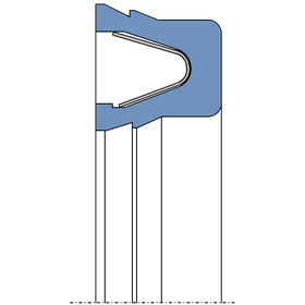
A rod/piston combined seal compatible with the P-number grooves of JIS B2401, suitable for use in harsh environments. It has low friction and excellent heat and chemical resistance.
- Other machine elements
- Other semiconductor manufacturing equipment
- Sealing
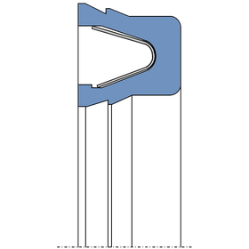
A seal with excellent chemical resistance that maintains the cleanliness of the semiconductor manufacturing environment.
- Other machine elements
- Other semiconductor manufacturing equipment
- Sealing
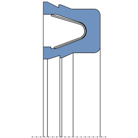
To the chemical industry pursuing chemical resistance. Achieving both chemical resistance and low friction.
- Other machine elements
- Other semiconductor manufacturing equipment
- Sealing
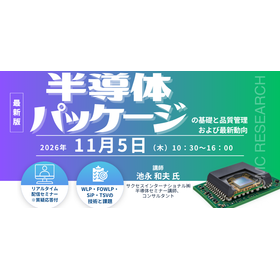

Systematically acquire semiconductor packaging technology from the basics. Learn about quality control and the latest packaging trends in one day.
- Technical Seminar
- Other semiconductor manufacturing equipment
- Other semiconductors
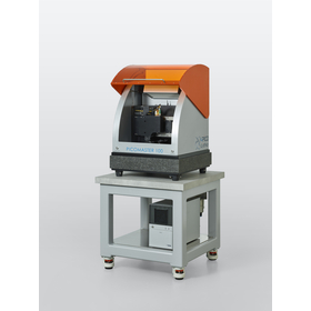

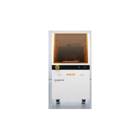
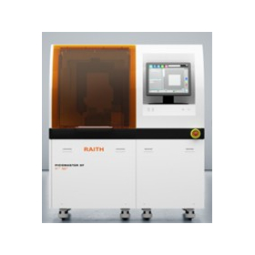
Achieving ultra-fine high-resolution drawing on the tabletop.
- Other semiconductor manufacturing equipment
- Electron beam lithography equipment


High-performance, cost-effective RF/DC magnetron sputtering device for research and development.
- Other semiconductor manufacturing equipment
- Sputtering Equipment

4-Yen Multi-Sputtering Device 【MiniLab-S060】
4 cathodes with Φ2 inch configuration Simultaneous film deposition: 3-component simultaneous deposition (RF 500W or DC 850W) + HiPIMS (PulseDC 5KW) x 1 Power distribution and configuration settings for 4 cathodes can be freely changed via the HMI screen using the plasma relay switch 3 MFC systems (Ar, O2, N2) for reactive sputtering RIE etching stage RF 300W (main chamber) + <30W soft etching (LL chamber) Substrate heating: Max 500℃, 800℃, or 1000℃ (C/C or SiC coating) Substrate rotation and vertical movement (automatically controlled by stepping motor) APC automatic control: Upstream (MFC flow adjustment) or downstream (automatic valve opening adjustment on the exhaust side) Dimensions: 1,120(W) x 800(D) ● Mixed specifications for resistance heating deposition, organic material deposition, EB deposition, PECVD, etc. are also possible.
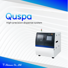

We propose a custom-made dispenser that fulfills your ideals.
- Other semiconductor manufacturing equipment
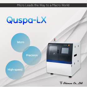
Significantly reduce tact time with continuous dispensing! The ultra-precision dispenser device 'Quspa-LX' enables high-precision fine dispensing.
- Other semiconductor manufacturing equipment

Notice of Exhibited Products and Events for Nepcon Japan 2024
We are pleased to announce that Shinwa will be exhibiting at the Internepcon Japan, which will be held from January 24 to January 26. Date: January 24 (Wed) - January 26 (Fri) 10:00 AM - 5:00 PM Location: Tokyo Big Sight, East Hall 1 Booth Number: [E4-8B] At our booth, we will be showcasing the newly redesigned dispenser device "Quspa-LX" for the first time. You will be able to see a demonstration. Additionally, we will introduce the TXC Corporation's crystal oscillators, which hold the number one global market share, and the CMOS camera modules for automotive applications from the Foxconn Group. On January 25 (Thu), the famous YouTuber Monozukuri Taro will be appearing at our booth! He will clearly explain the appeal of our new products. There will be two sessions on that day, so don't miss this opportunity! Morning: 11:00 AM Afternoon: 3:00 PM We look forward to seeing you there. Please note that pre-registration is required for entry to Internepcon Japan this year. If you have not registered, please do so via the link.

CVD, PVD (evaporation, sputtering, etc.) high vacuum, ultra-high temperature plate heater for wafer and small chip heating with excellent uniformity and reproducibility.
- Other semiconductor manufacturing equipment
- Annealing furnace
- CVD Equipment

■□【PyroMini】□■ Compact High-Performance Infrared Temperature Sensor
High-performance touch panel converter for easy setup, data logging, and data storage on microSD card. The PM2.2 model can also measure glossy metal surfaces. 【Overview】 With a highly visible high-brightness touch panel display, parameters such as temperature range, emissivity, and sampling rate can be intuitively operated and set. Long-term data storage and management are possible with a microSD card. (*An option for a converter without a display is also available.) The compact sensor head, measuring φ18mm x 45mm, allows for temperature measurement in tight spaces. It employs sensors and cables with excellent noise resistance, making it suitable for integration into moving equipment such as robotic arms. The PM2.2 model uses a short wavelength of 2.2um, supporting high temperatures (Max 2000℃) and measurements of glossy metal material surfaces. 【Features】 ◎ Wide range: -20 to 1000℃ (PM), 100 to 2000℃ (PM2.2) ◎ Excellent basic performance: Accuracy ±1%, reproducibility ±0.5%, 240msec fast response ◎ Measurement wavelength range: 8 to 14μm (PM), 2.0 to 2.2μm (PM2.2) ◎ Compact Φ18mm x 45mm
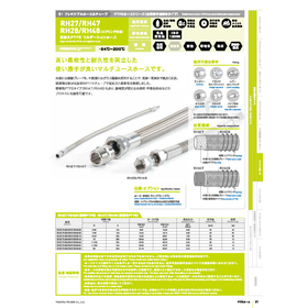

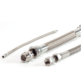
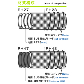
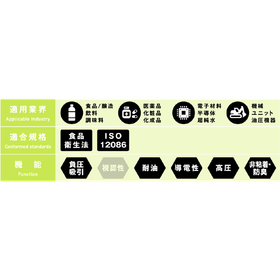
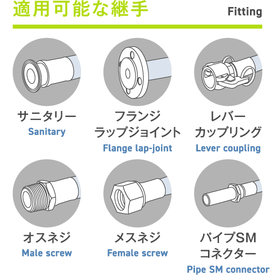
High-durability PTFE hoses achieve both high flexibility and durability through a fine wave PTFE structure. They are suitable for chemical supply lines and movable piping sections in semiconductor man...
- hose
- Other semiconductor manufacturing equipment
- Etching Equipment

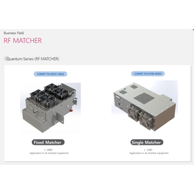
From RF solutions to repair and refurbishment. FNS supports semiconductor manufacturing as a whole.
- Other semiconductor manufacturing equipment
Compatible with 2 to 12-inch wafers. Customizable for each item.
- Other cleaning machines
- Other semiconductor manufacturing equipment
- Other semiconductors