
List of Semiconductor Manufacturing Equipment products
- classification:Semiconductor Manufacturing Equipment
91~135 item / All 5261 items


Reduce the workload from handling heavy objects! Here are five case studies that solved customer challenges! We are also accepting free consultations and tests tailored to your work!

- Other conveying machines


No more need to lift heavy one-gallon cans! Enjoy comfortable liquid transfer in the central kitchen.
- Other Pumps
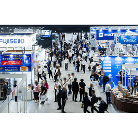
Decision to exhibit at the 1st Chubu Food Industry Creation Exhibition '26!
We will be exhibiting at the "1st Chubu Food Industry Creation Exhibition '26" to be held at Port Messe Nagoya from November 4 (Wednesday) to November 6 (Friday), 2026. As a new addition to our lineup, we will showcase the "Cordless Sanitary Handy Pump," which is a product we started selling in April last year, alongside our "Compact Sanitary Handy Pump Model MHS." - Cordless! Portable anywhere! Easy to use! Simple cleaning! It is compatible with standard 18L cans and BIB (Bag-in-Box) and features a structure that allows for easy disassembly and cleaning. We would like to invite you to visit us at this opportunity. - Venue: Port Messe Nagoya - Our exhibition booth: Hall 1 "C-66"
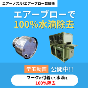

[Patent Obtained] Instant complete water removal of workpieces with air blow = complete drying!
- Other semiconductor manufacturing equipment

Revolutionary! No need for water washing! Particles are removed with just air blow.
- Other semiconductor manufacturing equipment
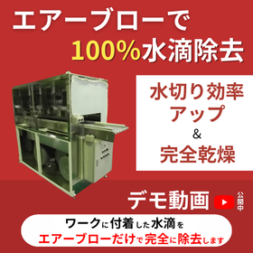
Are you making this mistake when draining water from your work?
- Other semiconductor manufacturing equipment


Are you making this mistake with the work's drainage?


- Other semiconductor manufacturing equipment

Are you making this mistake while draining water from the work?
[To those in charge who are struggling with workpiece water drainage] Are you making these mistakes with workpiece water drainage? ✓ Do you know the real reason why, even if you increase the air blow pressure, not all water droplets are blown away? ✓ Do you know the real reason why, even if you increase the number of air nozzles, water is not sufficiently drained? ✓ Do you know the real reason why, even if you change the shape of the air nozzle, it still does not drain water effectively? These mistakes are typical errors made by companies that use air blow for workpiece water drainage and droplet removal. However, these mistakes are not significant compared to a certain "fatal mistake." What is that "fatal mistake"? It is… We provide this information in a PDF file. Download it now to find out.

No more revolution! No need for washing; particles are removed with just air blowing.


- Other semiconductor manufacturing equipment

Just by looking at this, you'll understand everything! We created a PR flyer (dust removal version).
Thoroughly remove dust from workpieces with air blow! We have summarized everything about the patented complete dust removal air nozzle, "Air Screw Nozzle," on a single A4 flyer. "What kind of nozzle is it?" "Why can it remove dust so effectively?" "How can it remove dust even from complex-shaped workpieces?" Just by looking at this, you can quickly understand everything about the Air Screw Nozzle. Please download and take a look.

[Patent Obtained] Complete water removal in an instant with air blow = complete drying!


- Other semiconductor manufacturing equipment

If you see this, you'll understand everything! I created a PR flyer.
100% water removal with air blow! No water droplets left on the workpiece! We have summarized everything about the patented complete drying air nozzle, "Air Screw Nozzle," on a single A4 flyer. "What kind of nozzle is it?" "Can it really remove 100% of the water?" "Why is it so effective at removing water?" Just by looking at this, you can quickly understand everything about the Air Screw Nozzle. Please download it and take a look!


A unique LED UV curing solution with numerous patents obtained! Applying UV resin curing in electronics, industry, medical, and optics!
- Other semiconductor manufacturing equipment
- LED Module
- Ultraviolet irradiation equipment
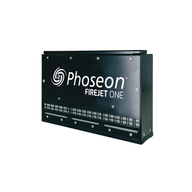
Expanding UV LED products to strengthen response to the growing and diversifying needs for ultraviolet curing.
Excelsius Noble Light Japan Co., Ltd. (Headquarters: Bunkyo-ku, Tokyo, President: Masahiko Suzuki, hereinafter referred to as "the Company") will expand its product portfolio of UV LEDs, one of the light sources for UV curing, and strengthen the provision of UV curing process solutions in new growth areas. In January 2024, the Company was absorbed by Excelsius Technologies, headquartered in the United States (hereinafter referred to as "Excelsius"), and is now handling UV LED products previously managed by its predecessor, Heraeus Noblelight Japan Co., Ltd., and Foseon Technology Japan Co., Ltd., as well as Excelsius. These products encompass a wide range of UV LED light sources for line and area irradiation as well as spot irradiation, regardless of cooling methods. As market demands become increasingly diverse, the Company has established a system that enables more detailed proposals to a broad range of industries through this product expansion.
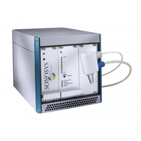

Thorough removal of fine contaminants from wafers. High-quality cleaning achieved by Sonosys.
- Ultrasonic Cleaner
- Ultrasonic Oscillator
- Photomask
[Exhibition Information] SONOSYS from Germany will exhibit at "SEMICON Japan 2026".
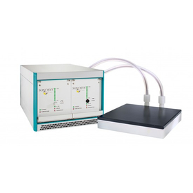
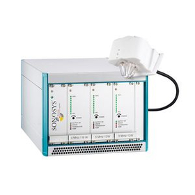
We are pleased to announce that SONOSYS, a German manufacturer represented by our company, will be exhibiting at "SEMICON Japan 2026," which will be held at Tokyo Big Sight, utilizing the "EU Business Hub" program to support EU companies entering the Japanese market. SONOSYS provides megasonic cleaning technology suitable for cleaning processes of semiconductor wafers, MEMS, and precision electronic components. At this exhibition, representatives from SONOSYS will be visiting Japan from Germany to introduce their megasonic cleaning technology. 【Exhibition Overview】 Exhibition Name: SEMICON Japan 2026 Dates: December 9 (Wednesday) - 11 (Friday), 2026 Venue: Tokyo Big Sight Exhibiting Company: SONOSYS (Germany) Participation Program: EU Business Hub Booth Number: Details will be provided as soon as they are finalized. If you are interested in the removal of fine particles in semiconductor manufacturing processes or reducing damage during cleaning, please take this opportunity to see SONOSYS's technology. Our company is also collaborating with SONOSYS to provide consultations regarding megasonic cleaning technology.
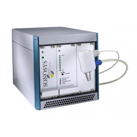
For precise cleaning of prisms. Sonosys ultrasonic cleaning device.
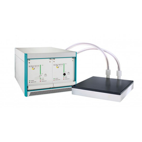
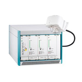
- Ultrasonic Cleaner
- Ultrasonic Oscillator
- Photomask
[Exhibition Information] SONOSYS from Germany will exhibit at "SEMICON Japan 2026".
We are pleased to announce that SONOSYS, a German manufacturer represented by our company, will be exhibiting at "SEMICON Japan 2026," which will be held at Tokyo Big Sight, utilizing the "EU Business Hub" program to support EU companies entering the Japanese market. SONOSYS provides megasonic cleaning technology suitable for cleaning processes of semiconductor wafers, MEMS, and precision electronic components. At this exhibition, representatives from SONOSYS will be visiting Japan from Germany to introduce their megasonic cleaning technology. 【Exhibition Overview】 Exhibition Name: SEMICON Japan 2026 Dates: December 9 (Wednesday) - 11 (Friday), 2026 Venue: Tokyo Big Sight Exhibiting Company: SONOSYS (Germany) Participation Program: EU Business Hub Booth Number: Details will be provided as soon as they are finalized. If you are interested in the removal of fine particles in semiconductor manufacturing processes or reducing damage during cleaning, please take this opportunity to see SONOSYS's technology. Our company is also collaborating with SONOSYS to provide consultations regarding megasonic cleaning technology.

Flow spray of 2 mmlit/min or less is possible!
- nozzle
- valve
- Etching Equipment

Start of distribution of 3D CAD data for Sonia Corporation's ultrasonic spray nozzle.
We have started distributing 3D CAD data for the Sonia ultrasonic spray nozzles. Designers and equipment manufacturers can efficiently proceed with equipment design and layout considerations by confirming product shapes and mounting dimensions in advance. This time, we have also released the 3D CAD data for the ultrasonic spray nozzles "WS40K" and "WS130K," which can be used for interference checks and design simulations before implementation. Sonia's ultrasonic spray nozzles cater to a wide range of applications, including precision coating, surface treatment, humidification, and cleaning. By providing 3D CAD data, we support the reduction of design man-hours and the shortening of development periods, facilitating a smooth process from product selection to equipment development.

Atomization of liquid without pressurization by piezo vibration. Enables uniform application while reducing power consumption and liquid waste.


- spray
- Coating Machine
- CMP Equipment
Start of distribution of 3D CAD data for Sonia Corporation's ultrasonic spray nozzle.
We have started distributing 3D CAD data for the Sonia ultrasonic spray nozzles. Designers and equipment manufacturers can efficiently proceed with equipment design and layout considerations by confirming product shapes and mounting dimensions in advance. This time, we have also released the 3D CAD data for the ultrasonic spray nozzles "WS40K" and "WS130K," which can be used for interference checks and design simulations before implementation. Sonia's ultrasonic spray nozzles cater to a wide range of applications, including precision coating, surface treatment, humidification, and cleaning. By providing 3D CAD data, we support the reduction of design man-hours and the shortening of development periods, facilitating a smooth process from product selection to equipment development.
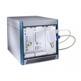
Leave the latest ultrasonic cleaning to Sonosys.


- Photomask
- CMP Equipment
- CVD Equipment
[Exhibition Information] SONOSYS from Germany will exhibit at "SEMICON Japan 2026".
We are pleased to announce that SONOSYS, a German manufacturer represented by our company, will be exhibiting at "SEMICON Japan 2026," which will be held at Tokyo Big Sight, utilizing the "EU Business Hub" program to support EU companies entering the Japanese market. SONOSYS provides megasonic cleaning technology suitable for cleaning processes of semiconductor wafers, MEMS, and precision electronic components. At this exhibition, representatives from SONOSYS will be visiting Japan from Germany to introduce their megasonic cleaning technology. 【Exhibition Overview】 Exhibition Name: SEMICON Japan 2026 Dates: December 9 (Wednesday) - 11 (Friday), 2026 Venue: Tokyo Big Sight Exhibiting Company: SONOSYS (Germany) Participation Program: EU Business Hub Booth Number: Details will be provided as soon as they are finalized. If you are interested in the removal of fine particles in semiconductor manufacturing processes or reducing damage during cleaning, please take this opportunity to see SONOSYS's technology. Our company is also collaborating with SONOSYS to provide consultations regarding megasonic cleaning technology.

Next-generation megasonic technology can instantly clear wafers up to 300mm.
- Photomask
- Other semiconductor manufacturing equipment
- Ultrasonic Cleaner
[Exhibition Information] SONOSYS from Germany will exhibit at "SEMICON Japan 2026".
We are pleased to announce that SONOSYS, a German manufacturer represented by our company, will be exhibiting at "SEMICON Japan 2026," which will be held at Tokyo Big Sight, utilizing the "EU Business Hub" program to support EU companies entering the Japanese market. SONOSYS provides megasonic cleaning technology suitable for cleaning processes of semiconductor wafers, MEMS, and precision electronic components. At this exhibition, representatives from SONOSYS will be visiting Japan from Germany to introduce their megasonic cleaning technology. 【Exhibition Overview】 Exhibition Name: SEMICON Japan 2026 Dates: December 9 (Wednesday) - 11 (Friday), 2026 Venue: Tokyo Big Sight Exhibiting Company: SONOSYS (Germany) Participation Program: EU Business Hub Booth Number: Details will be provided as soon as they are finalized. If you are interested in the removal of fine particles in semiconductor manufacturing processes or reducing damage during cleaning, please take this opportunity to see SONOSYS's technology. Our company is also collaborating with SONOSYS to provide consultations regarding megasonic cleaning technology.
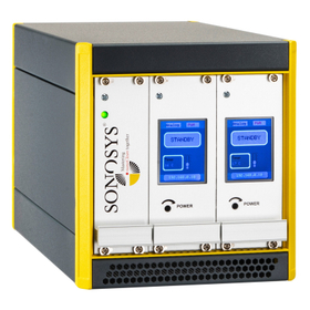
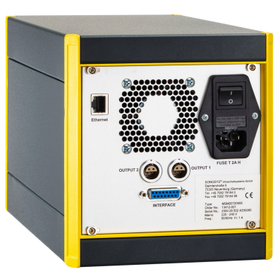
The Digital Generator is a digital control generator compatible with megasonic cleaning systems for semiconductors, electronic components, and precision instruments.
- Photomask
- Other semiconductor manufacturing equipment
- Wafer
[Exhibition Information] SONOSYS from Germany will exhibit at "SEMICON Japan 2026".
We are pleased to announce that SONOSYS, a German manufacturer represented by our company, will be exhibiting at "SEMICON Japan 2026," which will be held at Tokyo Big Sight, utilizing the "EU Business Hub" program to support EU companies entering the Japanese market. SONOSYS provides megasonic cleaning technology suitable for cleaning processes of semiconductor wafers, MEMS, and precision electronic components. At this exhibition, representatives from SONOSYS will be visiting Japan from Germany to introduce their megasonic cleaning technology. 【Exhibition Overview】 Exhibition Name: SEMICON Japan 2026 Dates: December 9 (Wednesday) - 11 (Friday), 2026 Venue: Tokyo Big Sight Exhibiting Company: SONOSYS (Germany) Participation Program: EU Business Hub Booth Number: Details will be provided as soon as they are finalized. If you are interested in the removal of fine particles in semiconductor manufacturing processes or reducing damage during cleaning, please take this opportunity to see SONOSYS's technology. Our company is also collaborating with SONOSYS to provide consultations regarding megasonic cleaning technology.


We provide high-quality circuit processing and wiring processing services using FIB. We achieve a high processing yield!
- Semiconductor inspection/test equipment
- Semiconductors and ICs
- Microcomputer
Supply disruptions from semiconductor manufacturers, the electrification of the automotive industry, and the spread of 5G communication. Are you keeping up with the urgent need for alternative product evaluations, authenticity assessments, and failure analysis?
The spread of 5G communication, the electrification of the automotive industry, the intensification of US-China trade friction represented by certain semiconductor manufacturers leading to supply stoppages, and the rapid increase in digital products due to the impact of the COVID-19 pandemic are various social phenomena that are increasing the demand for semiconductors. Along with these developments, the acceleration of semiconductor supply risks is progressing. In addition to the adoption of new products, evaluation of existing and distributed products is also necessary... However, the personnel involved in new adoption and product evaluation are limited. Do you have any of these concerns? - Lack of know-how to evaluate semiconductor components - Want to evaluate alternative products but lack personnel and equipment - Want to use stock items and market products but have concerns about reliability - Unable to determine whether the delivered semiconductor products are counterfeit or genuine At Eurofins FQL, we leverage our years of experience in component evaluation and failure analysis to provide not only semiconductor evaluations but also failure analysis services. Additionally, we offer evaluations of distributed products to assist in determining the authenticity of counterfeit, imitation, or long-term stored items. Please feel free to contact us.


Visualize surface foreign substances, dirt, and scratches! It is well-received as a daily management tool for yield management, quality control, cleaning management, and hygiene management. *Demo unit...
- Visual Inspection Equipment
- Semiconductor inspection/test equipment
- Defect Inspection Equipment
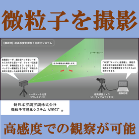
We will exhibit a particle visualization system at NIHONBASHI SPACE WEEK 2026. (December 1 (Tue) - December 3 (Thu), 2026 / Nihonbashi Mitsui Hall 1-40)
The particle visualization technology developed under our brand "ViEST" has a very high level of detection sensitivity, capable of visualizing the suspended and adhered states of micro and nano-sized particles in real-time. We are expanding our sales of visualization systems and providing evaluation services (investigating particles and airflow in production processes, inside and outside manufacturing equipment, assessing the performance of clean-up products, proposing yield improvement measures, etc.) both domestically and internationally. Shin Nihon Kucho introduces its efforts in air quality and airflow management, environmental control, and life support technology in space living environments. In addition to the "particle visualization technology" that visualizes particle behavior and airflow within space stations and lunar bases, we will showcase a "backwash filter" intended for the removal and collection of regolith, which poses challenges on the lunar surface. Furthermore, through displays that allow observation of regolith behavior in a vacuum environment, visitors can see how particles move in an environment different from that on Earth. We pursue the potential of technologies that control air and particles towards realizing a safe and comfortable living environment that supports human space activities.
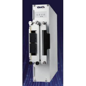
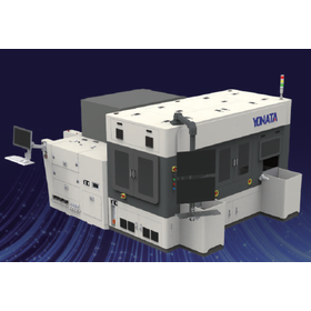
Cutting-edge testing systems supporting the AI era! Solutions that achieve semiconductor testing with technology and quality.
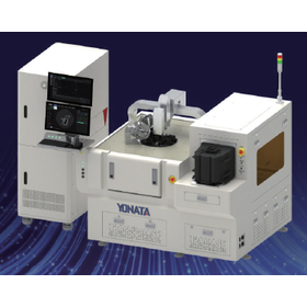
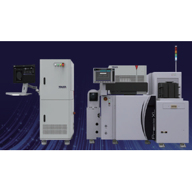
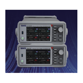
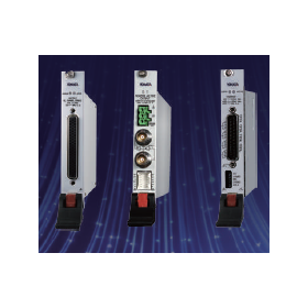
- Other semiconductors
- Semiconductor inspection/test equipment

High-precision horizontal (wet) device for PCM and PCB.
- Oxidation/Diffusion Device
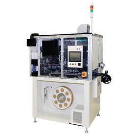

High-speed taping device: An automatic taping machine with a production capacity of 500 units per minute.
- Taping Machine
- Other semiconductor manufacturing equipment

Kyushu Measuring Instruments is the only authorized dealer in Japan.
- Ion implantation equipment


Compact, space-saving, energy-efficient! High-performance ultra-high temperature experimental furnace for R&D.
- Annealing furnace

■□【PyroMini】□■ Compact High-Performance Infrared Temperature Sensor
High-performance touch panel converter for easy setup, data logging, and data storage on microSD card. The PM2.2 model can also measure glossy metal surfaces. 【Overview】 With a highly visible high-brightness touch panel display, parameters such as temperature range, emissivity, and sampling rate can be intuitively operated and set. Long-term data storage and management are possible with a microSD card. (*An option for a converter without a display is also available.) The compact sensor head, measuring φ18mm x 45mm, allows for temperature measurement in tight spaces. It employs sensors and cables with excellent noise resistance, making it suitable for integration into moving equipment such as robotic arms. The PM2.2 model uses a short wavelength of 2.2um, supporting high temperatures (Max 2000℃) and measurements of glossy metal material surfaces. 【Features】 ◎ Wide range: -20 to 1000℃ (PM), 100 to 2000℃ (PM2.2) ◎ Excellent basic performance: Accuracy ±1%, reproducibility ±0.5%, 240msec fast response ◎ Measurement wavelength range: 8 to 14μm (PM), 2.0 to 2.2μm (PM2.2) ◎ Compact Φ18mm x 45mm
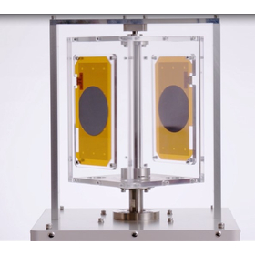

New concept cableless electrostatic chuck
- Other semiconductor manufacturing equipment
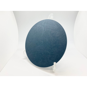
For stages and transport applications of processing machines and inspection equipment.
- Wafer processing/polishing equipment

Inline cleaning of particles on the stage - wafer-type stage cleaner
- Semiconductor inspection/test equipment
- Other semiconductor manufacturing equipment
- Other cleaning tools

Reduce positional displacement and measurement errors with low thermal expansion! Inverter/super inverter cutting plates for semiconductor manufacturing equipment and optical components.
- Other semiconductor manufacturing equipment
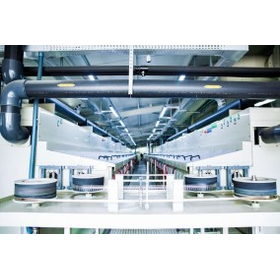

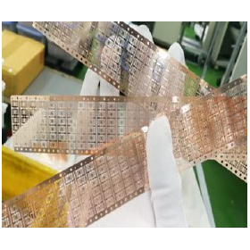
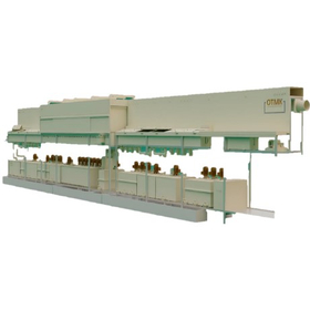
Unique technology to improve selectivity, productivity, and flexibility in the plating process!
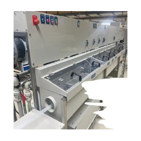
- Other semiconductor manufacturing equipment
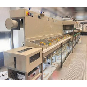
Precision plating using silver, gold, and palladium! Cutting-edge technology that achieves precise tolerances.
- Other semiconductor manufacturing equipment