1~4 item / All 4 items
Displayed results

Added to bookmarks
Bookmarks listBookmark has been removed
Bookmarks listYou can't add any more bookmarks
By registering as a member, you can increase the number of bookmarks you can save and organize them with labels.
Free membership registration
Contact this company
Inquiry Form1~4 item / All 4 items
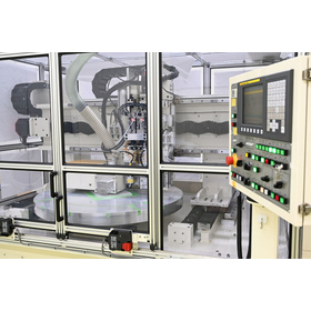
The CMP pad processing and inspection device "CMP1100S" is a dedicated processing device that performs high-precision surface processing of CMP pads used in the CMP (Chemical Mechanical Polishing) process. In semiconductor manufacturing, the condition of the CMP pad surface significantly affects polishing quality and processing accuracy. This device uniformly processes the CMP pad surface using unique processing technology, maintaining stable polishing performance. Furthermore, by combining it with the pad surface inspection device "INS800SA," it visualizes the surface condition after processing, providing consistent support for quality control. It can be widely utilized from research and development applications to mass production lines.
Added to bookmarks
Bookmarks listBookmark has been removed
Bookmarks listYou can't add any more bookmarks
By registering as a member, you can increase the number of bookmarks you can save and organize them with labels.
Free membership registration
The flatness processing device "CARE-TEC," developed by Toho Koki Co., Ltd., for next-generation semiconductor substrates, utilizes a new processing method that leverages catalytic action to efficiently and low-damage process high-hardness materials, including SiC (silicon carbide). *This is a product under development.* It suppresses processing damage and the occurrence of scratches, which have been challenges in conventional mechanical polishing, achieving excellent flatness and surface quality. It also contributes to cost reduction through shorter processing times and reduced usage of consumables. In addition to improving the efficiency of the processing steps, it also contributes to reducing environmental impact and manufacturing costs, accommodating a wide range of applications from research and development to mass production processes for next-generation power semiconductors. As a new flattening processing technology that realizes high quality, high productivity, and low cost, it supports productivity improvements in semiconductor manufacturing sites.
Added to bookmarks
Bookmarks listBookmark has been removed
Bookmarks listYou can't add any more bookmarks
By registering as a member, you can increase the number of bookmarks you can save and organize them with labels.
Free membership registration
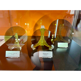
At Toho Steel Works, we handle single crystal SiC substrates and SiC bonded substrates for power semiconductors. Utilizing our unique procurement network, we also support the supply of SiC substrates from Chinese manufacturers, achieving high quality, low cost, and stable supply. For single crystal SiC substrates, we offer a wide range including ingots and 4-inch, 6-inch, and 8-inch substrates. With our dual bonding technology for SiC bonded substrates, we combine high-quality SiC layers with low-cost substrates to provide SiC substrates that achieve both high performance and cost reduction. Additionally, we welcome inquiries regarding the procurement of various semiconductor substrates, including SiC wafers, for both research and development and mass production applications. 【Features】 ■ We can propose products tailored to specific applications and specifications. ■ We can also support the sale of SiC substrates and related products from Chinese manufacturers. ■ In addition to SiC wafers, we handle a wide range of various semiconductor wafers and substrates.
Added to bookmarks
Bookmarks listBookmark has been removed
Bookmarks listYou can't add any more bookmarks
By registering as a member, you can increase the number of bookmarks you can save and organize them with labels.
Free membership registration
"CARE-TEC(R)" is a technology that dramatically improves device performance through ultimate flatness and damage-free processing. We use only environmentally friendly pure water as the processing fluid. Please feel free to contact us if you have any inquiries. 【Features】 ■ Achieves atomic-level flatness ■ Capable of removing processing damage (internal latent defects) ■ Can reduce leakage current *For more details, please download the PDF or contact us.
Added to bookmarks
Bookmarks listBookmark has been removed
Bookmarks listYou can't add any more bookmarks
By registering as a member, you can increase the number of bookmarks you can save and organize them with labels.
Free membership registration