Achieving high-efficiency and low-damage processing of SiC and GaN substrates (CARE device)

A next-generation semiconductor substrate flattening processing device that achieves both cost reduction and high quality for power semiconductor substrates! Realizing high-precision flattening processing while minimizing environmental impact.
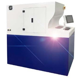
The flatness processing device "CARE-TEC," developed by Toho Koki Co., Ltd., for next-generation semiconductor substrates, utilizes a new processing method that leverages catalytic action to efficiently and low-damage process high-hardness materials, including SiC (silicon carbide). *This is a product under development.* It suppresses processing damage and the occurrence of scratches, which have been challenges in conventional mechanical polishing, achieving excellent flatness and surface quality. It also contributes to cost reduction through shorter processing times and reduced usage of consumables. In addition to improving the efficiency of the processing steps, it also contributes to reducing environmental impact and manufacturing costs, accommodating a wide range of applications from research and development to mass production processes for next-generation power semiconductors. As a new flattening processing technology that realizes high quality, high productivity, and low cost, it supports productivity improvements in semiconductor manufacturing sites.

Inquire About This Product
basic information
【Features】 ■ Adopts unique CARE (Catalyst-Referred Etching) processing technology ■ Supports high-precision flattening processing of high-hardness semiconductor substrates such as SiC ■ Significantly reduces processing damage and scratches ■ Achieves high-quality surface roughness ■ Reduces manufacturing costs through improved processing efficiency ■ Decreases the amount of consumables used ■ Contributes to reducing environmental impact ■ Broadly supports from research and development to mass production 【Recommended for】 ■ Those who want to improve the processing quality of SiC substrates ■ Those who want to reduce processing costs ■ Those who want to minimize processing damage ■ Those who want to improve productivity ■ Those who want to implement processing technology for next-generation semiconductors
Price range
Delivery Time
Applications/Examples of results
【Applications】 SiC (Silicon Carbide) wafers Next-generation power semiconductor substrates Flattening processing of semiconductor materials Precision processing of high-hardness materials Semiconductor research and development Semiconductor manufacturing lines Universities and research institutions Electronic materials manufacturers, etc.
catalog(1)
Download All Catalogs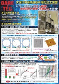
Company information

Our company is engaged in the processing of SiC and GaN substrates, other substrate processing, semiconductor CMP pad processing, manufacturing of pad processing equipment, and manufacturing of pad inspection equipment. Additionally, we perform polishing of SiC and GaN substrates using the CARE method. Please feel free to contact us if you have any inquiries.




![[Semiconductor/Class 100 Compatible] 100% Water-Free Air Nozzle](https://image.mono.ipros.com/public/product/image/2116982/IPROS15202438644694791694.png?w=280&h=280)