46~59 item / All 59 items
Displayed results
Filter by category
Added to bookmarks
Bookmarks listBookmark has been removed
Bookmarks listYou can't add any more bookmarks
By registering as a member, you can increase the number of bookmarks you can save and organize them with labels.
Free membership registration
Contact this company
Inquiry FormBefore making an inquiry
Download Profile46~59 item / All 59 items
Filter by category
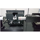
The high-precision "Camshaft Appearance Inspection Device" measures the height shape of the camshaft using a light sectioning method and detects the height compared to a processed reference camshaft. It compares the height with the reference camshaft of the original material to detect defects, connecting three measurement cameras in a one-to-one configuration to a single central PC for measurement. For more details, please download the catalog.
Added to bookmarks
Bookmarks listBookmark has been removed
Bookmarks listYou can't add any more bookmarks
By registering as a member, you can increase the number of bookmarks you can save and organize them with labels.
Free membership registrationThe high-speed inspection "ITO film appearance inspection device" measures the line width and conducts appearance inspections of transparent films on film and glass substrates. By using a special optical system, it clearly captures the presence or absence of transparent patterns such as touch panel ITO films and detects splatter for appearance measurement. For more details, please download the catalog.
Added to bookmarks
Bookmarks listBookmark has been removed
Bookmarks listYou can't add any more bookmarks
By registering as a member, you can increase the number of bookmarks you can save and organize them with labels.
Free membership registrationThe high-speed measurement "Seal Displacement Measurement Device" quickly measures the gap dimensions between the seal area and the BM area of the LCD glass panel. The transport is continuous, and by using a CCD camera to capture still images with a strobe light, it enables high-speed and stable measurements with inexpensive transport machinery. For more details, please download the catalog.
Added to bookmarks
Bookmarks listBookmark has been removed
Bookmarks listYou can't add any more bookmarks
By registering as a member, you can increase the number of bookmarks you can save and organize them with labels.
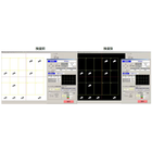
Free membership registrationThe "Wire Bonding Inspection Device" for model teaching displays images of ideal samples that have been captured, allowing for the specification of inspection positions and test measurements to be conducted with simple mouse operations using the set parameters. Results such as wire trajectories are visually displayed, making verification easy. For more details, please download the catalog.
Added to bookmarks
Bookmarks listBookmark has been removed
Bookmarks listYou can't add any more bookmarks
By registering as a member, you can increase the number of bookmarks you can save and organize them with labels.
Free membership registrationThe inspection device "Wafer Edge Appearance Inspection Machine" simultaneously inspects defects such as scratches, foreign objects, and cracks on the edge and three surfaces (top and bottom) of the wafer through high-speed optical image inspection. (The inspection time for an 8” wafer is 6 seconds, making it very fast.) The wafer is adhered to the back side, and its shape is recognized by the camera to detect outer diameter eccentricity and the position/amount of the orifice, which controls the inspection machine. The newly developed triple optical system and integrated lighting have enabled detailed image inspection of the edge. External PIO control is also possible, allowing it to be integrated into automated systems. It can accommodate wafer sizes from 4 inches to 8 inches. For more details, please download the catalog.
Added to bookmarks
Bookmarks listBookmark has been removed
Bookmarks listYou can't add any more bookmarks
By registering as a member, you can increase the number of bookmarks you can save and organize them with labels.
Free membership registrationThe inspection device "Pattern Inspection Device" registers a normal surface as a master and detects foreign substances, scratches, dirt, and pattern defects by comparing the registered image during inspection. It also displays the position of the alignment pattern and performs dimensional inspections. The area and size (maximum diameter) of the detected patterns and foreign substances are measured, and the inspection result data is compared with measurement conditions to determine good or defective products. The inspection result data is filed and stored. For more details, please download the catalog.
Added to bookmarks
Bookmarks listBookmark has been removed
Bookmarks listYou can't add any more bookmarks
By registering as a member, you can increase the number of bookmarks you can save and organize them with labels.
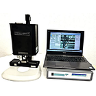
Free membership registrationThe inspection device "cp-30 (microscope-type image measurement system)" is a system that analyzes images captured by a CCD camera attached to a microscope to automatically measure line widths. It precisely measures line widths from the brightness waveform of horizontal or vertical windows set within the screen. It is linked with an XY stage through a dedicated interface, allowing it to automatically move to specified positions for width measurement. The Z-axis autofocus function enables flexible handling of workpieces with varying thicknesses. Additionally, a wafer loader and unloader can also be installed. For more details, please download the catalog.
Added to bookmarks
Bookmarks listBookmark has been removed
Bookmarks listYou can't add any more bookmarks
By registering as a member, you can increase the number of bookmarks you can save and organize them with labels.
Free membership registrationThe inspection device "Foreign Object Inspection Device" processes images captured by a camera using inspection software (Ip-20), allowing for various analyses to be conducted at high speed. The high degree of freedom in selecting camera models as input sources is a significant feature of this system. It is compatible with most commercially available NTSC and digital output cameras, enabling flexible inline device configurations ranging from high-end, high-functionality devices to low-cost, widely-used models. For more details, please download the catalog.
Added to bookmarks
Bookmarks listBookmark has been removed
Bookmarks listYou can't add any more bookmarks
By registering as a member, you can increase the number of bookmarks you can save and organize them with labels.
Free membership registrationThe inspection device "Transparent Film Inspection Certification Device" allows for direct visual observation or camera observation of patterns such as transparent films formed on transparent glass with high contrast. It generates a backlight effect that uniformly diffuses light on the surface of the glass substrate beyond the critical angle, preventing edges from glowing white when compared to dark field illumination. By incorporating coaxial reflective lighting with adjusted light intensity, it suppresses the scattering surface reflection of the transparent glass section and enhances the halation effect, increasing the reflectivity in areas without the transparent film due to the transmission effect. This makes it possible to improve the contrast by darkening the pattern of the transparent electrode under backlight. For more details, please download the catalog.
Added to bookmarks
Bookmarks listBookmark has been removed
Bookmarks listYou can't add any more bookmarks
By registering as a member, you can increase the number of bookmarks you can save and organize them with labels.
Free membership registrationThe inspection device "Glass Substrate Outline Inspection Device (PSI-50)" is capable of measuring outer dimensions (maximum width), detecting burrs, detecting chips, inspecting cutting misalignment, and measuring the dimensions of the glass pouring section. It also features a measurement MAP display function and image storage, among others. Additionally, with the automatic angle correction function for the panel, there is no need to precisely align the angle when placing the workpiece on the inspection stage. Once installed, it automatically corrects the angle. If the placed angle is too large, it will affect measurement accuracy, and an alarm will be displayed. For more details, please download the catalog.
Added to bookmarks
Bookmarks listBookmark has been removed
Bookmarks listYou can't add any more bookmarks
By registering as a member, you can increase the number of bookmarks you can save and organize them with labels.
Free membership registration
The Super Macro SM75 can inspect 300mm wafers in one shot in just one second, making it suitable for fully automated inspection lines due to its short inspection time. It is available with a lineup of optical systems for small fields of view, and by using infrared as an optional light source, it can also be applied to internal void inspections. For more details, please contact us or download the catalog.
Added to bookmarks
Bookmarks listBookmark has been removed
Bookmarks listYou can't add any more bookmarks
By registering as a member, you can increase the number of bookmarks you can save and organize them with labels.
Free membership registration
"Aerofix" is a vacuum chuck developed using a unique ceramic sintering technology, which takes a completely different approach from conventional through-hole type vacuum chucks. By controlling the eutectic reaction between the main agent and the auxiliary agent, it manages sinterability, adjusting to the optimal pore diameter and porosity for the workpiece. Additionally, since it is fully sintered during the manufacturing process, there is no dust generation from within, ensuring it does not affect the working environment. Previously, it was necessary to design and manufacture chuck devices tailored to the shape of the workpiece, but the "Aerofix," which allows for partial adsorption, can accommodate various workpiece sizes. There is no need to prepare different types and sizes for each workpiece, leading to cost reduction and improved work efficiency. It generates uniform adsorption force, making it safe to use even for delicate thin workpieces. Moreover, it can also adsorb edge warps seen in films, enhancing work efficiency (touchdown). The adsorption force can be adjusted using a vacuum pressure control valve. We offer demonstration units for "Aerofix." Please experience the exceptional performance of our product firsthand. For more details, please contact us or download the catalog.
Added to bookmarks
Bookmarks listBookmark has been removed
Bookmarks listYou can't add any more bookmarks
By registering as a member, you can increase the number of bookmarks you can save and organize them with labels.
Free membership registration
Arrows Engineering designs, manufactures, modifies, repairs, and sells peripheral equipment for semiconductor devices, undertakes construction related to semiconductor manufacturing equipment, and manufactures and sells momentary voltage drop protection devices. We introduce repair and improvement services for items such as "high-frequency power supplies," "RF matching boxes," and "transport robots." We also list the models we support for repairs. Our company accurately captures customer needs and provides suitable support, helping to resolve various issues swiftly with reliable technology and advanced knowledge. [Repair and Improvement Details] ■ High-Frequency Power Supply: Improvement of heat dissipation ■ RF Matching Box: Regular replacement of overloaded or aging parts to stabilize RF matching functionality and enhance durability ■ Repair of Transport Robots: Disassembly of robots and controllers, wafer transport testing ■ Repair of PCB Boards: Repair of PCB boards from various equipment manufacturers *For more details, please refer to the PDF document or feel free to contact us.
Added to bookmarks
Bookmarks listBookmark has been removed
Bookmarks listYou can't add any more bookmarks
By registering as a member, you can increase the number of bookmarks you can save and organize them with labels.
Free membership registrationArrows Engineering Co., Ltd. has been involved in the semiconductor business since its establishment in 1986, and we strive to be an indispensable company in the semiconductor industry by accurately capturing our customers' needs. With the desire to continue being essential, all our employees work daily to provide the highest quality products, technologies, and services. We assist in solving various problems with reliable technology and advanced knowledge, accurately addressing our customers' needs and providing optimal support. For more details, please contact us or refer to our catalog.
Added to bookmarks
Bookmarks listBookmark has been removed
Bookmarks listYou can't add any more bookmarks
By registering as a member, you can increase the number of bookmarks you can save and organize them with labels.
Free membership registration