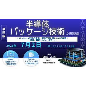
7/2 Basic Course on Semiconductor Packaging Technology WEB Seminar
 CMC RESEARCH Ltd.
Title: "Fundamentals of Semiconductor Packaging Technology
~ From the Evolution of Package Types to Manufacturing Processes, Equipment and Materials Used, and Latest Trends ~"
This is an introductory seminar where you can systematically learn about semiconductor packaging technology from the basics to advanced techniques. It provides a clear explanation of the role of packaging technology that supports the high performance of semiconductors, its background of evolution, manufacturing processes, and materials and equipment technologies. In addition to the characteristics of various package types such as DIP, QFP, BGA, and WLCSP, it also details major manufacturing technologies like back grinding, dicing, die bonding, wire bonding, and molding. Furthermore, you will learn about the trends and future prospects of the latest technologies such as SiP, FOWLP, CoWoS, EMIB, chiplets, and optoelectronic integrated packaging. This content is ideal for semiconductor engineers as well as sales and marketing personnel who want to understand packaging technology from the ground up.
| Date and time | Thursday, Jul 02, 2026 |
|---|---|
| Entry fee | Charge Tuition fee: 44,000 yen (including tax) *Price for our newsletter subscribers (registration is free): 39,600 yen (including tax) |
Inquiry about this news
Contact Us OnlineMore Details & Registration
Details & Registration
Related product
Distributors