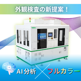
[Semiconductor/Wafer Inspection] AI × Full-Color Image Inspection Device AURCA
AURCA series

For manufacturing sites troubled by excessive detection. This inspection device accurately determines fine defects in wafers through AI analysis and full-color image inspection, achieving improved yield.
■Do you face these challenges in semiconductor and wafer inspection? - You cannot afford to miss tiny defects, but excessive detection is common, leading to lower yield. - It is difficult to balance efficiency and accuracy in the inspection process. The image inspection device 'AURCA' equipped with AI analysis capabilities solves these challenges. 【Reasons to Choose AURCA / Differences from Competitors】 ▼Overwhelming inspection accuracy with AI analysis × full color Tiny scratches and unevenness that were difficult to distinguish with conventional monochrome images can be accurately identified by combining full-color images with advanced AI analysis. The accuracy of distinguishing between good and defective products dramatically improves. ▼Reduce setup time with auto-focus function Automatically adjusts focus according to the object. This shortens the setup time and allows for high-resolution inspections under optimal conditions at all times. 【Benefits of Implementation】 - Significantly reduce excessive detection and improve the yield of semiconductor substrates. - Decrease reliance on visual inspections, achieving stabilization of quality and cost reduction. The catalog includes detailed product specifications, the mechanism of AI analysis, and detection capability data. Please use it as a reference for comparison during your evaluation of implementation.
Inquire About This Product
basic information
For more details, please check the PDF by downloading the "Catalog" below, or feel free to contact us.
Price range
Delivery Time
Applications/Examples of results
For more details, please check the PDF by downloading the "Catalog" below or feel free to contact us.
catalog(2)
Download All Catalogs
Company information

Our inspection target areas include printed circuit boards, semiconductor packages, and display panels. These are core components of information and communication devices that are growing increasingly due to advancements in IT, as well as widely adopted digital home appliances. Printed circuit boards, semiconductor packages, and display panels are evolving at an astonishing speed, and higher precision technologies are required in inspections. Our company holds a significant share in these inspection fields that demand cutting-edge technology, and we have delivered numerous products recognized as "de facto standards" in the industry worldwide.