iPROS Manufacturing
  • Search for products by classification category

    • Electronic Components and Modules
      Electronic Components and Modules
      61465items
    • Machinery Parts
      Machinery Parts
      75691items
    • Manufacturing and processing machinery
      Manufacturing and processing machinery
      101701items
    • Scientific and Physics Equipment
      Scientific and Physics Equipment
      36175items
    • Materials
      Materials
      37664items
    • Measurement and Analysis
      Measurement and Analysis
      55369items
    • Image Processing
      Image Processing
      15344items
    • Control and Electrical Equipment
      Control and Electrical Equipment
      54286items
    • Tools, consumables, and supplies
      Tools, consumables, and supplies
      65291items
    • Design and production support
      Design and production support
      12650items
    • IT/Network
      IT/Network
      45365items
    • Office
      Office
      14129items
    • Business support services
      Business support services
      25204items
    • Seminars and Skill Development
      Seminars and Skill Development
      6536items
    • Pharmaceutical and food related
      Pharmaceutical and food related
      33600items
    • others
      74984items
  • Search for companies by industry

    • Manufacturing and processing contract
      7327
    • others
      4978
    • Industrial Machinery
      4436
    • Machine elements and parts
      3316
    • Other manufacturing
      2885
    • Trading company/Wholesale
      2609
    • IT/Telecommunications
      2556
    • Industrial Electrical Equipment
      2315
    • Building materials, supplies and fixtures
      1815
    • software
      1656
    • Electronic Components and Semiconductors
      1576
    • Resin/Plastic
      1500
    • Service Industry
      1458
    • Testing, Analysis and Measurement
      1131
    • Ferrous/Non-ferrous metals
      985
    • environment
      698
    • Chemical
      637
    • Automobiles and Transportation Equipment
      574
    • Printing Industry
      512
    • Information and Communications
      464
    • Consumer Electronics
      411
    • Energy
      327
    • Rubber products
      318
    • Food Machinery
      307
    • Optical Instruments
      277
    • robot
      272
    • fiber
      253
    • Paper and pulp
      229
    • Pharmaceuticals and Biotechnology
      172
    • Electricity, Gas and Water Industry
      165
    • Warehousing and transport related industries
      149
    • Glass and clay products
      139
    • Food and Beverage
      130
    • CAD/CAM
      123
    • retail
      109
    • Medical Devices
      106
    • Educational and Research Institutions
      103
    • Ceramics
      98
    • wood
      88
    • Transportation
      82
    • Petroleum and coal products
      62
    • Medical and Welfare
      61
    • Shipbuilding and heavy machinery
      50
    • Aviation & Aerospace
      47
    • Fisheries, Agriculture and Forestry
      41
    • equipment
      38
    • Public interest/special/independent administrative agency
      31
    • Materials
      29
    • Research and development equipment and devices
      27
    • Government
      24
    • self-employed
      24
    • Mining
      17
    • Finance, securities and insurance
      13
    • cosmetics
      13
    • Individual
      10
    • Restaurants and accommodations
      9
    • Police, Fire Department, Self-Defense Forces
      7
    • Laboratory Equipment and Consumables
      5
    • Raw materials for reagents and chemicals
      3
    • Contracted research
      3
  • Special Features
  • Ranking

    • Overall Products Ranking
    • Overall Company Ranking
Search for Products
  • Search for products by classification category

  • Electronic Components and Modules
  • Machinery Parts
  • Manufacturing and processing machinery
  • Scientific and Physics Equipment
  • Materials
  • Measurement and Analysis
  • Image Processing
  • Control and Electrical Equipment
  • Tools, consumables, and supplies
  • Design and production support
  • IT/Network
  • Office
  • Business support services
  • Seminars and Skill Development
  • Pharmaceutical and food related
  • others
Search for Companies
  • Search for companies by industry

  • Manufacturing and processing contract
  • others
  • Industrial Machinery
  • Machine elements and parts
  • Other manufacturing
  • Trading company/Wholesale
  • IT/Telecommunications
  • Industrial Electrical Equipment
  • Building materials, supplies and fixtures
  • software
  • Electronic Components and Semiconductors
  • Resin/Plastic
  • Service Industry
  • Testing, Analysis and Measurement
  • Ferrous/Non-ferrous metals
  • environment
  • Chemical
  • Automobiles and Transportation Equipment
  • Printing Industry
  • Information and Communications
  • Consumer Electronics
  • Energy
  • Rubber products
  • Food Machinery
  • Optical Instruments
  • robot
  • fiber
  • Paper and pulp
  • Pharmaceuticals and Biotechnology
  • Electricity, Gas and Water Industry
  • Warehousing and transport related industries
  • Glass and clay products
  • Food and Beverage
  • CAD/CAM
  • retail
  • Medical Devices
  • Educational and Research Institutions
  • Ceramics
  • wood
  • Transportation
  • Petroleum and coal products
  • Medical and Welfare
  • Shipbuilding and heavy machinery
  • Aviation & Aerospace
  • Fisheries, Agriculture and Forestry
  • equipment
  • Public interest/special/independent administrative agency
  • Materials
  • Research and development equipment and devices
  • Government
  • self-employed
  • Mining
  • Finance, securities and insurance
  • cosmetics
  • Individual
  • Restaurants and accommodations
  • Police, Fire Department, Self-Defense Forces
  • Laboratory Equipment and Consumables
  • Raw materials for reagents and chemicals
  • Contracted research
Special Features
Ranking
  • Overall Products Ranking
  • Overall Company Ranking
  • privacy policy
  • terms of service
  • About Us
  • Careers
  • Advertising
  1. Home
  2. Industrial Machinery
  3. ニデックアドバンステクノロジー 本社、東京営業所、名古屋営業所
  4. Product/Service List
Industrial Machinery
  • Added to bookmarks

    Bookmarks list

    Bookmark has been removed

    Bookmarks list

    You can't add any more bookmarks

    By registering as a member, you can increase the number of bookmarks you can save and organize them with labels.

    Free membership registration

ニデックアドバンステクノロジー 本社、東京営業所、名古屋営業所

EstablishmentNovember 25, 1991
capital93800Ten thousand
number of employees303
addressKyoto/Muko-shi/Nidec Park 33
phone075-280-8100
  • Special site
  • Official site
last updated:Jun 24, 2026
ニデックアドバンステクノロジーlogo
  • Contact this company

    Inquiry Form
  • Company information
  • Products/Services(40)
  • catalog(58)
  • news(4)

ニデックアドバンステクノロジー Product Lineup

  • category

1~40 item / All 40 items

Displayed results

Filter by category

Visual Inspection Equipment Visual Inspection Equipment
Electrical Inspection Equipment Electrical Inspection Equipment
Power semiconductor Inspection Equipment Power semiconductor Inspection Equipment
Inspection Fixture Inspection Fixture
Automotive measuring instruments for EVs Automotive measuring instruments for EVs
Probe Card Related Probe Card Related
class="retina-image"

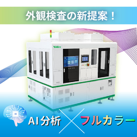
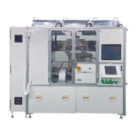
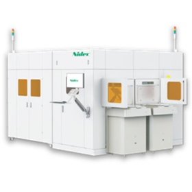
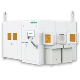
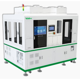
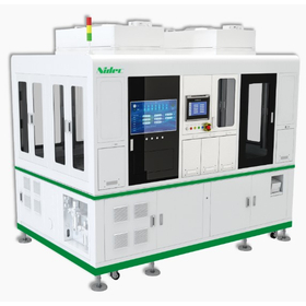
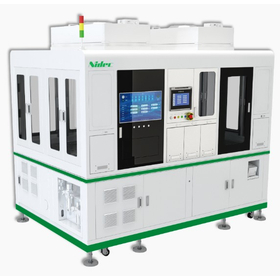
[Semiconductor/Wafer Inspection] AI × Full-Color Image Inspection Device AURCA

For manufacturing sites troubled by excessive detection. This inspection device accurately determines fine defects in wafers through AI analysis and full-color image inspection, achieving improved yield.

■Do you face these challenges in semiconductor and wafer inspection? - You cannot afford to miss tiny defects, but excessive detection is common, leading to lower yield. - It is difficult to balance efficiency and accuracy in the inspection process. The image inspection device 'AURCA' equipped with AI analysis capabilities solves these challenges. 【Reasons to Choose AURCA / Differences from Competitors】 ▼Overwhelming inspection accuracy with AI analysis × full color Tiny scratches and unevenness that were difficult to distinguish with conventional monochrome images can be accurately identified by combining full-color images with advanced AI analysis. The accuracy of distinguishing between good and defective products dramatically improves. ▼Reduce setup time with auto-focus function Automatically adjusts focus according to the object. This shortens the setup time and allows for high-resolution inspections under optimal conditions at all times. 【Benefits of Implementation】 - Significantly reduce excessive detection and improve the yield of semiconductor substrates. - Decrease reliance on visual inspections, achieving stabilization of quality and cost reduction. The catalog includes detailed product specifications, the mechanism of AI analysis, and detection capability data. Please use it as a reference for comparison during your evaluation of implementation.

  • Semiconductor inspection/test equipment
  • Wafer
  • Circuit Board Inspection Equipment

Added to bookmarks

Bookmarks list

Bookmark has been removed

Bookmarks list

You can't add any more bookmarks

By registering as a member, you can increase the number of bookmarks you can save and organize them with labels.

Free membership registration

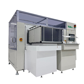
Semiconductor tester for high-speed testing of MLCCs and IPDs.

Expansion of measurement conditions and built-in 64 LCR meters enable faster and more accurate inspections!

Our "R-5920MK2" and "R-5940A" are multi-pin high-speed testers that achieve overwhelming efficiency and speed in the inspection of electronic components such as MLCCs (Multi-Layer Ceramic Capacitors) and IPDs (Integrated Passive Devices). We offer two new models tailored to our customers' inspection needs. 【R5920MK2】 ■ 4W inspection speed increase: Added "designated point output pull-in function" to the scanning unit for reliable judgment in bulk. ■ Improved contamination cleaning function: Cleaning current can be freely modulated and controlled from 100mA to 200mA. ■ Simultaneous parallel inspection with 64 LCR meters: LCR meters are directly built into the scanner card itself. ■ Significant increase in measurement speed: Achieved faster capacitance measurement speed compared to conventional testers. ■ Supports measurement of direct current consumption: Capable of controlling MEMS microphone ICs, allowing for measurement of power consumption.

  • Tester
  • Semiconductor inspection/test equipment
  • Circuit Board Inspection Equipment

Added to bookmarks

Bookmarks list

Bookmark has been removed

Bookmarks list

You can't add any more bookmarks

By registering as a member, you can increase the number of bookmarks you can save and organize them with labels.

Free membership registration

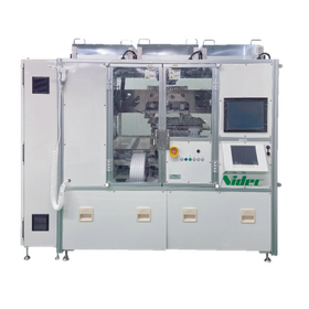
High-precision inspection equipment for large individual semiconductor packages.

Overall positioning accuracy ±2.5µm! A high-precision inspection device ideal for inspecting large, multi-pin semiconductor package substrates.

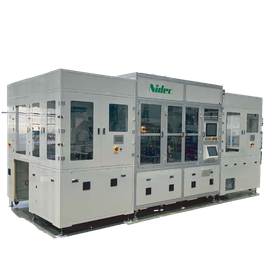
"GATS-7837" is a high-precision inspection device that achieves extremely high contact accuracy in the inspection of semiconductor package substrates, which are increasing in size and pin count. 【Features】 ■ Overall positioning accuracy ±2.5μm ■ Loader/unloader support for tray insertion/removal *For more details, please download the PDF or feel free to contact us.

  • Semiconductor inspection/test equipment
  • Other inspection equipment and devices
  • Circuit Board Inspection Equipment

Added to bookmarks

Bookmarks list

Bookmark has been removed

Bookmarks list

You can't add any more bookmarks

By registering as a member, you can increase the number of bookmarks you can save and organize them with labels.

Free membership registration

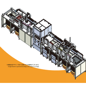
Large substrate HDI through-insulation inspection device 'GATS8360'

Supports a maximum of 112Kp up and down! Achieving multi-pin and high-precision inspection of large HDI boards.

This is a high-precision conductive insulation inspection device that supports reliable quality assurance for large HDI substrates. 【Features】 ■ Supports a maximum inspection point count of 112Kp ■ High-precision inspection for large HDI ■ Overall alignment accuracy of ±3.5μm ■ Compatible with the new tester series R-5920MK2 We offer two models that can be selected according to your application (work size and accuracy). Please feel free to contact us for any inquiries regarding specifications.

  • Semiconductor inspection/test equipment
  • Other semiconductor manufacturing equipment
  • Circuit Board Inspection Equipment

Added to bookmarks

Bookmarks list

Bookmark has been removed

Bookmarks list

You can't add any more bookmarks

By registering as a member, you can increase the number of bookmarks you can save and organize them with labels.

Free membership registration

Semiconductor package multi-surface full panel substrate inspection device

Support for a total of 48K points in both vertical and horizontal directions! A high-speed inspection solution for multi-panel arrangements of large full-panel PCBs (500×620mm).

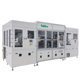
We would like to introduce our semiconductor package multi-site full panel substrate inspection equipment, the 'GATS-8370'. It is optimal for next-generation semiconductor packages with larger unit sizes and more pins. This high-precision electrical inspection device supports bulk and high-speed inspection of full panel substrates. It achieves efficient step-and-repeat inspection with a single shuttle, balancing quality improvement and reduced takt time. 【Features】 ■ Comprehensive inspection with a large capacity of 48K points (49,152p) ■ Bulk inspection of large unit products (up to 300mm) ■ Compatible with large full panel sizes (500mm × 620mm) *For more details, please download the PDF or feel free to contact us.

  • Semiconductor inspection/test equipment
  • Circuit Board Inspection Equipment

Added to bookmarks

Bookmarks list

Bookmark has been removed

Bookmarks list

You can't add any more bookmarks

By registering as a member, you can increase the number of bookmarks you can save and organize them with labels.

Free membership registration

TGV Through Hole Glass Substrate Inspection Device

The optimal imaging inspection device for TGV inspection has been completed!

By using high-resolution 2D and 3D cameras, and combining them with NIR (near-infrared), we have achieved the detection of all types of defects. In addition to conventional high-precision surface inspection, it is now possible to measure internal defects and depth using NIR. Furthermore, the range of compatible materials has expanded beyond just glass to include SiC/silicon wafers, ABF films, and more. Please feel free to contact us.

  • Printed Circuit Board
  • Semiconductor inspection/test equipment
  • Visual Inspection Equipment

Added to bookmarks

Bookmarks list

Bookmark has been removed

Bookmarks list

You can't add any more bookmarks

By registering as a member, you can increase the number of bookmarks you can save and organize them with labels.

Free membership registration

NS PROBE Miniaturization and Advanced Shapes

A probe that realizes miniaturization and diversification of advanced shapes using MEMS processes!

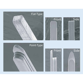
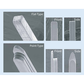
We would like to introduce our product, the "NS Probe." This is a product for inspection systems for printed circuit boards and semiconductor package substrates. It has achieved miniaturization and diversification of advanced shapes using MEMS processes. We offer two types of Probe: "Flat" and "Point." Please feel free to contact us when you need assistance. 【Features】 ■Flat-Type - Improved dimensional accuracy ■Point-Type - Material selection available *For more details, please download the PDF or feel free to contact us.

  • Electron tube
  • probe
  • Circuit Board Inspection Equipment

Added to bookmarks

Bookmarks list

Bookmark has been removed

Bookmarks list

You can't add any more bookmarks

By registering as a member, you can increase the number of bookmarks you can save and organize them with labels.

Free membership registration

Electrical testing for semiconductor package substrates - full panel size inspection available.

Full panel size support! A high-capacity, high-speed, and high-precision inspection solution compatible with a maximum point count of 24Kch.

We would like to introduce our high-speed and high-precision inspection equipment for semiconductor packages, the 'GATS-7885'. This electrical inspection system achieves high-speed and high-precision probing for electrical testing of FOPLP/RDL using glass carriers. 【Features】 ■ Capable of inspecting full panel size (510×515 mm) ■ Supports up to 24K channels on the upper side ■ Overall alignment accuracy of ±3.5 μm ■ Capable of two types of RSD inspections ■ Compliant with SEMI standards *For more details, please download the PDF or feel free to contact us.

  • Semiconductor inspection/test equipment

Added to bookmarks

Bookmarks list

Bookmark has been removed

Bookmarks list

You can't add any more bookmarks

By registering as a member, you can increase the number of bookmarks you can save and organize them with labels.

Free membership registration

Automated Transport System "EFEM Series"

Equipment Front End Module Full Panel Size Compatible Automatic Transporter

Introducing the Equipment Front End Module full panel size compatible automatic transport system "EFEM Series." The "EFEM Series" is an automatic transport system compatible with full panel sizes (510×515mm/600×600mm). It utilizes robots manufactured by our group company, Nidec Instruments, and can be customized in various ways to meet customer needs! Please feel free to contact us.

  • Substrate transport device (loader/unloader)
  • Transport and handling robots
  • Circuit Board Inspection Equipment

Added to bookmarks

Bookmarks list

Bookmark has been removed

Bookmarks list

You can't add any more bookmarks

By registering as a member, you can increase the number of bookmarks you can save and organize them with labels.

Free membership registration

High-speed and high-precision inspection device for semiconductor packages 'GATS-7785'

Full panel size support! A high-capacity, high-speed, and high-precision inspection solution compatible with a maximum point count of 24Kch.

We would like to introduce our high-speed and high-precision inspection equipment for semiconductor packages, the 'GATS-7885'. This electrical inspection system achieves high-speed and high-precision probing for electrical testing of FOPLP/RDL using glass carriers. 【Features】 ■ Capable of inspecting full panel size (510×515 mm) ■ Supports up to 24K channels on the upper side ■ Overall alignment accuracy of ±3.5 μm ■ Capable of two types of RSD inspections ■ Compliant with SEMI standards *For more details, please download the PDF or feel free to contact us.

  • Semiconductor inspection/test equipment

Added to bookmarks

Bookmarks list

Bookmark has been removed

Bookmarks list

You can't add any more bookmarks

By registering as a member, you can increase the number of bookmarks you can save and organize them with labels.

Free membership registration

Conductive Inspection Device "STAR REC V6"

Large-scale / Multi-pin Board Continuity Insulation Testing Equipment

Introducing the "STAR REC V6" series, a conductive insulation testing device for large/multi-pin boards currently under development. The "STAR REC V6" is equipped with our latest high-precision, high-speed tester, achieving a comprehensive alignment accuracy of ±10μm. It also meets the inspection needs of larger and multi-point boards! If you are having trouble with stacking or handling large boards, we can accommodate the supply and discharge to board storage trays, as well as transportation with AGVs. Please feel free to consult with us!

  • Defect Inspection Equipment
  • Circuit Board Inspection Equipment
  • Other inspection equipment and devices

Added to bookmarks

Bookmarks list

Bookmark has been removed

Bookmarks list

You can't add any more bookmarks

By registering as a member, you can increase the number of bookmarks you can save and organize them with labels.

Free membership registration

MEMS spring probe

Achieving the production of the world's smallest class springs!

We have achieved the production of the world's smallest class springs through our unique patented technology. We have developed a vertical MEMS spring probe combined with ultra-small plungers. These can be incorporated into fixtures for PCB inspection and probe cards, and are suitable for electrical testing of semiconductors and printed circuit boards. In addition to the ability to select the tip shape of the DUT plunger, we can meet your desired load and stroke through custom design. Please feel free to contact us.

  • probe
  • Inspection fixture
  • Circuit Board Inspection Equipment

Added to bookmarks

Bookmarks list

Bookmark has been removed

Bookmarks list

You can't add any more bookmarks

By registering as a member, you can increase the number of bookmarks you can save and organize them with labels.

Free membership registration

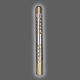
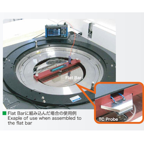
TC-Probe

Device temperature measurement probe

Thermocouple technology has been applied to the probe! It is possible to accurately measure the temperature of the DUT!

  • Semiconductor inspection/test equipment

Added to bookmarks

Bookmarks list

Bookmark has been removed

Bookmarks list

You can't add any more bookmarks

By registering as a member, you can increase the number of bookmarks you can save and organize them with labels.

Free membership registration

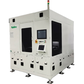
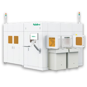
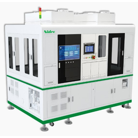
Equipped with an autofocus mechanism! Image inspection device "AURCA Series"

Equipped with an autofocus mechanism to prevent distortion blur! Image inspection device "AURCA Series"

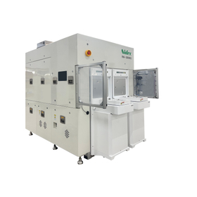
The AI-equipped appearance inspection device series "AURCA" for electronic circuit boards and semiconductor silicon wafers is equipped with an autofocus mechanism (AF) that enables quick and accurate focusing. ■ Features - Full-color high-speed line scan - Equipped with autofocus mechanism (prevents blurring due to warping) - Integrated detection of AI + conventional algorithms (hybrid inspection) - Minimizes miss rate and false detection rate to the extreme - Automatic classification and quantitative measurement of defects (length, width, area, position) - Inspection time reduced by over 30% (supports high throughput mass production) ■ Example Inspection Items - RDL defect inspection: open, short, notch, metal residue, CD variation - Bump defect inspection: surface anomalies, dimensional deviations, missing/position misalignment - TSV defect inspection: metal and foreign material contamination, deformation, dimensional deviations - Other appearance defects: edge chipping, adhesive residue, dents, foreign materials, scratches, oxidation, corrosion, film cracks, bright spots

  • Defect Inspection Equipment
  • Visual Inspection Equipment
  • Circuit Board Inspection Equipment

Added to bookmarks

Bookmarks list

Bookmark has been removed

Bookmarks list

You can't add any more bookmarks

By registering as a member, you can increase the number of bookmarks you can save and organize them with labels.

Free membership registration

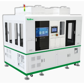
RDL defect inspection, bump defect inspection, TSV defect inspection compatible appearance inspection equipment.

The sale of the appearance inspection device "AURCA series," which supports RDL defect inspection, bump defect inspection, and TSV defect inspection, has begun!

The AURCA series is a next-generation 2D appearance inspection system that combines full-color high-speed scanning with AI technology, compatible with wafers and panels. It features full-color line scanning and an autofocus mechanism, integrating conventional image processing (CV) with AI algorithms. In mass production lines, it simultaneously achieves high detection rates, low false detection, and high-speed processing. ■ Features - Full-color high-speed line scanning - Equipped with an autofocus mechanism (prevents blurriness due to warping) - Integrated detection of AI and conventional algorithms (hybrid inspection) - Minimizes miss rate and excessive detection rate to the extreme - Automatic classification and quantitative measurement of defects (length, width, area, position) - Reduces inspection time by over 30% (supports high throughput mass production) ■ Example Inspection Items - RDL defect inspection: open, short, notch, metal residue, CD variation - Bump defect inspection: surface anomalies, dimensional deviations, missing/position misalignment - TSV defect inspection: metal and foreign object contamination, deformation, dimensional deviations - Other appearance defects: edge chipping, adhesive residue, dents, foreign objects, scratches, oxidation, corrosion, film cracks, bright spots

  • Wafer
  • Visual Inspection Equipment
  • Defect Inspection Equipment

Added to bookmarks

Bookmarks list

Bookmark has been removed

Bookmarks list

You can't add any more bookmarks

By registering as a member, you can increase the number of bookmarks you can save and organize them with labels.

Free membership registration

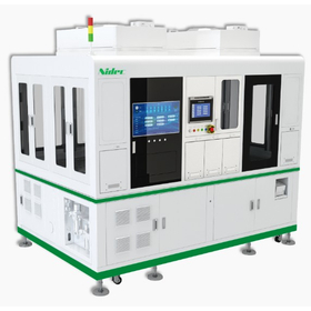
AI-equipped visual inspection device for semiconductor wafers and panels "AURCA Series"

The AI-equipped appearance inspection device "AURCA Series" for semiconductor wafers and panels has arrived! It can also inspect semiconductor package substrates and printed circuit boards!

The AURCA-S series is a 2D appearance inspection device that combines full-color high-speed scanning with high-precision AI analysis. It is designed to accommodate the increasingly fine inspection of wafers in recent years. ■ Features - Full-color high-speed line scanning - Equipped with an autofocus mechanism (prevents blurring due to warping) - Integrated detection with AI and conventional algorithms (hybrid inspection) - Minimizes miss rate and false detection rate to the extreme - Automatic classification and quantitative measurement of defects (length, width, area, position) - Inspection time reduced by over 30% (supports high throughput mass production) ■ Example Inspection Items - RDL defect inspection: open, short, notch, metal residue, CD variation - Bump defect inspection: surface anomalies, dimensional deviations, missing/position misalignment - TSV defect inspection: metal and foreign material contamination, deformation, dimensional deviations - Other appearance defects: edge chipping, adhesive residue, dents, foreign materials, scratches, oxidation, corrosion, film cracks, bright spots

  • Wafer
  • Visual Inspection Equipment
  • Defect Inspection Equipment

Added to bookmarks

Bookmarks list

Bookmark has been removed

Bookmarks list

You can't add any more bookmarks

By registering as a member, you can increase the number of bookmarks you can save and organize them with labels.

Free membership registration

Image inspection device for semiconductor package substrates "AURCA Series"

The "AURCA Series" image inspection device for semiconductor package substrates has arrived! It can also inspect printed circuit boards and wafers!

The AURCA series is a next-generation 2D appearance inspection system that integrates full-color high-speed scanning with AI technology, designed for high-density package substrates. With full-color imaging and a multi-effect optical configuration, it accurately captures a variety of defect characteristics. Furthermore, it goes beyond mere defect detection; the AI analysis function allows for the analysis of the shape and causes of detected defects! It supports the review of previous processes and the formulation of measures to prevent recurrence. ■ Features - Full-color high-speed line scan - Equipped with an autofocus mechanism (prevents blurring due to warping) - Integrated detection of AI and conventional algorithms (hybrid inspection) - Minimizes miss rate and false detection rate to the extreme - Automatic classification and quantitative measurement of defects (length, width, area, position) - Reduces inspection time by over 30% (supports high throughput mass production) ■ Example Inspection Items - RDL defect inspection: open, short, notch, metal residue, CD variation - Bump defect inspection: surface anomalies, dimensional deviations, missing/position misalignment - TSV defect inspection: metal and foreign matter contamination, deformation, dimensional deviations - Other appearance defects: edge chipping, adhesive residue, dents, foreign matter, scratches, oxidation, corrosion, film cracks, bright spots

  • Defect Inspection Equipment
  • Visual Inspection Equipment
  • Circuit Board Inspection Equipment

Added to bookmarks

Bookmarks list

Bookmark has been removed

Bookmarks list

You can't add any more bookmarks

By registering as a member, you can increase the number of bookmarks you can save and organize them with labels.

Free membership registration

Printed Circuit Board Image Inspection Equipment "AURCA Series"

AI inspection and measurement solution for printed circuit boards, image inspection device "AURCA Series"

■Features - Full-color high-speed line scan - Equipped with an autofocus mechanism (prevents blurring due to warping) - AI + conventional algorithm integrated detection (hybrid inspection) - Minimizes missed detection and excessive detection rates to the extreme - Automatic classification and quantitative measurement of defects (length, width, area, position) - Inspection time reduced by over 30% (supports high throughput mass production) ■Examples of inspection items - RDL defect inspection: open, short, notch, metal residue, CD variation - Bump defect inspection: surface anomalies, dimensional deviations, missing/position misalignment - TSV defect inspection: metal and foreign object contamination, deformation, dimensional deviations - Other appearance defects: edge chipping, adhesive residue, dents, foreign objects, scratches, oxidation, corrosion, film cracks, bright spots

  • Defect Inspection Equipment
  • Visual Inspection Equipment
  • Circuit Board Inspection Equipment

Added to bookmarks

Bookmarks list

Bookmark has been removed

Bookmarks list

You can't add any more bookmarks

By registering as a member, you can increase the number of bookmarks you can save and organize them with labels.

Free membership registration

Electronic circuit board and semiconductor silicon wafer inspection equipment "AURCA Series"

AI inspection and measurement solution for electronic circuit boards and semiconductor silicon wafers: Introducing the "AURCA Series" appearance inspection equipment!

The "AURCA series" is the latest inspection solution that addresses challenges in manufacturing, such as detecting defects that were difficult to identify with conventional image inspection methods and improving yield, all at once. Please make use of it in your quality improvement cycle! ■ Features - Full-color high-speed line scan - Equipped with an autofocus mechanism (prevents blurring due to warping) - Integrated detection of AI + conventional algorithms (hybrid inspection) - Minimizes missed detection and excessive detection rates to the extreme - Automatic classification and quantitative measurement of defects (length, width, area, position) - Reduces inspection time by over 30% (supports high throughput mass production) ■ Example of inspection items - RDL defect inspection: open, short, notch, metal residue, CD variation - Bump defect inspection: surface anomalies, dimensional deviations, missing/position misalignment - TSV defect inspection: metal and foreign material contamination, deformation, dimensional deviations - Other appearance defects: edge chipping, adhesive residue, dents, foreign materials, scratches, oxidation, corrosion, film cracks, bright spots

  • Defect Inspection Equipment
  • Visual Inspection Equipment
  • Circuit Board Inspection Equipment

Added to bookmarks

Bookmarks list

Bookmark has been removed

Bookmarks list

You can't add any more bookmarks

By registering as a member, you can increase the number of bookmarks you can save and organize them with labels.

Free membership registration

Appearance inspection device "AURCA series" contributing to yield improvement.

Appearance inspection device "AURCA series" contributing to yield improvement.

The "AURCA series" is an AI-equipped visual inspection device that not only conducts inspections but also continuously cycles through analysis → feedback → process improvement, contributing to the maximization of yield across the entire factory for our customers. Additionally, by analyzing the root causes of defects, it helps reduce manufacturing costs and improve product reliability by decreasing the number of defective products. ■ Features - Full-color high-speed line scan - Equipped with an autofocus mechanism (prevents blurring due to warping) - Integrated detection of AI and conventional algorithms (hybrid inspection) - Minimizes missed detection and excessive detection rates to the extreme - Automatic classification and quantitative measurement of defects (length, width, area, position) - Inspection time reduced by over 30% (supports high throughput mass production) ■ Example Inspection Items - RDL defect inspection: open, short, notch, metal residue, CD variation - Bump defect inspection: surface anomalies, dimensional deviations, missing/position misalignment - TSV defect inspection: metal and foreign material contamination, deformation, dimensional deviations - Other appearance defects: edge chipping, adhesive residue, dents, foreign materials, scratches, oxidation, corrosion, film cracks, bright spots

  • Defect Inspection Equipment
  • Circuit Board Inspection Equipment
  • Visual Inspection Equipment

Added to bookmarks

Bookmarks list

Bookmark has been removed

Bookmarks list

You can't add any more bookmarks

By registering as a member, you can increase the number of bookmarks you can save and organize them with labels.

Free membership registration

Full-color appearance inspection device "AURCA Series"

Full-color appearance inspection device "AURCA Series"

The AURCA series accurately captures changes in the material and height of objects through full-color image acquisition enabled by advanced optical design, significantly reducing over-detection. Defects that were difficult to identify with conventional monochrome images can now be detected! ■ Features - Full-color high-speed line scan - Equipped with an autofocus mechanism (prevents blurring due to warping) - Integrated detection using AI + traditional algorithms (hybrid inspection) - Minimizes miss rates and over-detection rates to the extreme - Automatic classification and quantitative measurement of defects (length, width, area, position) - Inspection time reduced by over 30% (supports high throughput mass production) ■ Example inspection items - RDL defect inspection: open, short, notch, metal residue, CD variation - Bump defect inspection: surface anomalies, dimensional deviations, missing/position misalignment - TSV defect inspection: metal and foreign material contamination, deformation, dimensional deviations - Other appearance defects: edge chipping, adhesive residue, dents, foreign materials, scratches, oxidation, corrosion, film cracks, bright spots

  • Semiconductor inspection/test equipment
  • Visual Inspection Equipment
  • Circuit Board Inspection Equipment

Added to bookmarks

Bookmarks list

Bookmark has been removed

Bookmarks list

You can't add any more bookmarks

By registering as a member, you can increase the number of bookmarks you can save and organize them with labels.

Free membership registration

AURCA Series

AI analysis function equipped!! Appearance inspection device

The launch of the next-generation AI visual inspection solution "AURCA Series" that visualizes invisible defects with AI has begun.

  • Visual Inspection Equipment
  • Defect Inspection Equipment
  • Circuit Board Inspection Equipment

Added to bookmarks

Bookmarks list

Bookmark has been removed

Bookmarks list

You can't add any more bookmarks

By registering as a member, you can increase the number of bookmarks you can save and organize them with labels.

Free membership registration

High-speed STEP & REPEAT type continuity and insulation testing equipment

Achieves the highest class of high-speed and high-precision inspection in the history of the M6 series. Ideal for HDI and IC package board inspection.
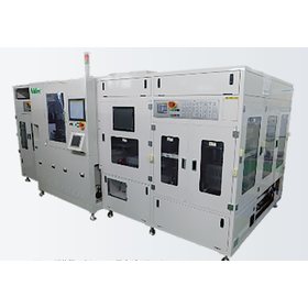
The "STAR REC M6V SW" is a high-performance appearance inspection device developed for HDI and IC substrates. It achieves the highest class of high-speed and high-precision inspection in the M6 series, strongly supporting quality assurance for electronic substrates as miniaturization and densification progress. With a high-resolution camera and proprietary image processing technology, it accurately detects even minute defects and abnormalities. By adopting a high-speed transport system, it also contributes to increased productivity. Additionally, it is compatible with automatic transport mechanisms, allowing for flexible adaptation to line automation and labor-saving measures. Furthermore, it combines excellent operability with stable inspection performance, accommodating a wide range from small lots of various types to mass production lines. It provides a high-quality and efficient inspection environment required for next-generation electronic device manufacturing.
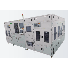
  • Circuit Board Inspection Equipment

Added to bookmarks

Bookmarks list

Bookmark has been removed

Bookmarks list

You can't add any more bookmarks

By registering as a member, you can increase the number of bookmarks you can save and organize them with labels.

Free membership registration

Large HDI substrate conductive insulation inspection device GATS

Supports high-density, multi-pin inspection. Achieves high-precision continuity and insulation testing for large HDI substrates and interposers.

The GATS-7885/8360A is a high-precision continuity insulation testing device developed for interposers and large HDI substrates. In addition to full-panel high-precision inspection, it also supports high-density, multi-pin testing and LCR testing, providing strong support for quality assurance of next-generation semiconductor packages and high-functionality substrates. The GATS-7885 is equipped with a dedicated fixture that supports up to 24K points and is compatible with small-diameter pad probes with a 25μm pitch. It can propose optimal fixture designs tailored to the pad layout. Furthermore, it achieves a comprehensive alignment accuracy of ±3.5μm, enabling stable high-precision inspections. The GATS-8360A, as a high-precision inspection device for large HDI, supports a maximum of 96K points inspection with 32K points on the upper side and 64K points on the lower side. It also accommodates various automation system proposals, supporting productivity improvement and labor reduction. It is the ideal solution for manufacturing environments that require high-precision and high-efficiency inspection.

  • Semiconductor inspection/test equipment

Added to bookmarks

Bookmarks list

Bookmark has been removed

Bookmarks list

You can't add any more bookmarks

By registering as a member, you can increase the number of bookmarks you can save and organize them with labels.

Free membership registration

Analysis support tool "Pulse EYE"

Instantly analyze desired characteristic results from R&D to mass production testing! Analysis of test data from other companies is also possible.

"Pulse EYE" is a support tool for the analysis of Power semiconductor testing and waveforms. It features various modes such as "Waveform Analyze," which allows for graph display and manipulation of arbitrary signals, cursor display, selection of analysis position display, and locus graph display functionality, as well as "Dual File View," which enables easy comparison display by overlaying graphs from two files. Please feel free to contact us if you have any inquiries. 【Features】 ■Improved work efficiency/time reduction ■Displays all waveforms in 2-3 seconds with one click ■Analysis position information display ■Comparison of multiple file displays ■Waveform display with black and white inversion *For more details, please download the PDF or feel free to contact us.

  • Other network tools

Added to bookmarks

Bookmarks list

Bookmark has been removed

Bookmarks list

You can't add any more bookmarks

By registering as a member, you can increase the number of bookmarks you can save and organize them with labels.

Free membership registration

TDAS Series <Performance Test/Durability Test>

Supports ultra-high speed of 36,000 rpm! Cameras and various sensors can also be connected, enabling time-axis synchronized logging.

The "TDAS-Series" is a device designed for performance and durability testing of onboard drive motors for EVs/HEVs, as well as E-Axles (integrated motor, inverter, and gear). With original measurement, control, and analysis software and GUI, it allows for simple operation to conduct various tests, including constant torque operation, constant speed operation, and tests tailored to driving patterns such as WLTC. Additionally, it enables real-time monitoring of images and data via a live camera, and remote monitoring through the TDAS monitoring system. 【Features】 ■ Capable of constructing 3-axis/4-axis test benches ■ Capable of constructing test benches for inverters ■ Measurement, control, and analysis possible with simple and easy operation ■ Compatible with TDAS remote monitoring system ■ Supports ultra-high speed of 36,000 rpm *For more details, please download the PDF or feel free to contact us.

  • Testing Equipment and Devices

Added to bookmarks

Bookmarks list

Bookmark has been removed

Bookmarks list

You can't add any more bookmarks

By registering as a member, you can increase the number of bookmarks you can save and organize them with labels.

Free membership registration

IGBT/SiC Power Module Inspection Equipment "NATS Series"

Low LS 4.5nH! Introducing Nidec Advance Technology's inspection equipment.

We would like to introduce our IGBT/SiC power module testing equipment, the 'NATS Series'. We offer the automatic testing device "NATS-1000," which achieves low LS values and supports high-precision testing for insulation, static characteristics, and dynamic characteristics, as well as the manual testing device "NATS-1630/1730," which can be integrated with external PCs and upper data management systems such as the cloud. Please feel free to contact us when you need assistance. 【Features】 <NATS-1000> ■ Insulation testing (ISO) ■ Static characteristics testing (DC) ■ Dynamic characteristics testing (AC) ■ High-temperature testing up to 175°C (up to 200°C) ■ High throughput of up to 144 UPH (25 seconds/unit) *For more details, please download the PDF or feel free to contact us.

  • Other inspection equipment and devices

Added to bookmarks

Bookmarks list

Bookmark has been removed

Bookmarks list

You can't add any more bookmarks

By registering as a member, you can increase the number of bookmarks you can save and organize them with labels.

Free membership registration

Wafer bump automatic inspection system 'RWi-300MK3'

Ideal for gold bump 3D inspection! Achieves simultaneous measurement of 3D/2D/SD with high speed and high precision.

We would like to introduce our high-speed, high-precision 3D/2D/SD wafer bump automatic inspection system, the 'RWi-300MK3'. The measurement accuracy for 2D/3D has significantly improved, enabling ultra-fast inspections. Additionally, the speed of defect image acquisition has dramatically increased. Please feel free to contact us if you require further information. 【Features】 ■ Simultaneous measurement of 3D/2D/SD achieved with high speed and high precision ■ Suitable for gold bump 3D inspection ■ Diverse transport systems *For more details, please download the PDF or feel free to contact us.

  • Other inspection equipment and devices

Added to bookmarks

Bookmarks list

Bookmark has been removed

Bookmarks list

You can't add any more bookmarks

By registering as a member, you can increase the number of bookmarks you can save and organize them with labels.

Free membership registration

3D Measurement Device "NSAT Series"

Technology and reliability compatible with glass core! High-speed, high-precision 3D measurement device.

We would like to introduce our 3D measurement device compatible with glass substrates, the 'NSAT Series.' It supports a depth of 5μm and a line space of 2/2. It offers various measurement functions such as Trace, Anchor, Overlay, and Film. Please feel free to contact us if you have any inquiries. 【Features】 ■ Supports depth of 5μm and line space of 2/2 ■ Thickness measurement of SR and ABF using transmission measurement method ■ Technical capability and reliability compatible with glass cores *For more details, please download the PDF or feel free to contact us.

  • Circuit Board Inspection Equipment

Added to bookmarks

Bookmarks list

Bookmark has been removed

Bookmarks list

You can't add any more bookmarks

By registering as a member, you can increase the number of bookmarks you can save and organize them with labels.

Free membership registration

NS Probe <Printed Circuit Board & Semiconductor Package Board Inspection>

A probe that achieves miniaturization and diversification of advanced shapes using MEMS processes!

We would like to introduce our product, the "NS Probe." This is a product for inspection systems for printed circuit boards and semiconductor package substrates. It has achieved miniaturization and diversification of advanced shapes using MEMS processes. We offer two types of Probe: "Flat" and "Point." Please feel free to contact us when you need assistance. 【Features】 ■ Flat-Type - Improved dimensional accuracy ■ Point-Type - Material selection is possible *For more details, please download the PDF or feel free to contact us.

  • probe

Added to bookmarks

Bookmarks list

Bookmark has been removed

Bookmarks list

You can't add any more bookmarks

By registering as a member, you can increase the number of bookmarks you can save and organize them with labels.

Free membership registration

High-precision inspection jig

A 4-terminal fixture for measuring small resistances! Compatible with fine conductors and electrode pads.

We would like to introduce our "high-precision inspection jigs" that we handle. Products for printed circuit board and semiconductor package inspection systems. They are compatible with fine conductors and electrode pads. We are also developing probes with diameters of 7um and 10um. Please feel free to contact us when needed. 【Features】 ■ One-touch jig ■ Probes with diameters of 7um and 10um in development ■ Four-terminal jig for measuring micro-resistance *For more details, please download the PDF or feel free to contact us.

  • Inspection fixture

Added to bookmarks

Bookmarks list

Bookmark has been removed

Bookmarks list

You can't add any more bookmarks

By registering as a member, you can increase the number of bookmarks you can save and organize them with labels.

Free membership registration

Continuity/Insulation Testing Tester 'RZ-1207'

Compatible with flat cables! Equipped with automatic mechanisms, manual mechanisms, and desktop mechanisms, etc.

We would like to introduce our continuity/insulation testing tester 'RZ-1207'. This advanced tester, compatible with flat cables, incorporates a wealth of optional features that can be added as needed. It is well-suited for testing circuit patterns on bare boards and flex circuits, as well as for harness inspections. Please feel free to contact us if you have any inquiries. 【Features】 ■ High speed and high precision ■ Scanner card ■ Up to 16k test points ■ 4W testing ■ μOPEN testing * For more details, please download the PDF or feel free to contact us.

  • Tester

Added to bookmarks

Bookmarks list

Bookmark has been removed

Bookmarks list

You can't add any more bookmarks

By registering as a member, you can increase the number of bookmarks you can save and organize them with labels.

Free membership registration

AC/DC MULTI TESTER "R-700 Series"

Micro-capacity inspection with high resolution! Capable of inspecting various products such as thin-film RF filters and accelerometers.

The "R-700 Series" is a compactly designed AC/DC MULTI TESTER that offers high speed and high precision. It can inspect various products such as thin-film RF filters, automotive DC modules, acceleration sensors, and MEMS devices. We offer a lineup including the "R-730 Standard," "R-780 High Insulation," and "R-770 AC Dynamic." 【Features】 ■ Ultra high insulation ■ High speed and high precision ■ Compact design ■ Maximum inspection points: 512 pins ■ High resolution for small capacitance measurement ■ 4W low resistance measurement: 0.1mΩ~ *For more details, please download the PDF or feel free to contact us.

  • Tester

Added to bookmarks

Bookmarks list

Bookmark has been removed

Bookmarks list

You can't add any more bookmarks

By registering as a member, you can increase the number of bookmarks you can save and organize them with labels.

Free membership registration

High-Speed OPEN/LEAK Tester "R-5940"

IC multi-function inspection support! Equipped with an LCR meter developed in-house.

The R-5940 is a super tester specialized for IC embedded substrates. It meets the diverse needs of high-precision IC testing with high-speed continuity and short-circuit measurements, μΩ accuracy, high-speed testing with four-terminal measurements, and all-CH LCR measurements. By connecting up to 16 SMUs as power supplies and electronic loads to the DUT, it enables the implementation of power ON/OFF sequences, allowing for DUT measurements with freely combined SMUs. 【Features】 ■ High-speed testing ■ High precision ■ Specialized for IC embedded *For more details, please download the PDF or feel free to contact us.

  • Tester

Added to bookmarks

Bookmarks list

Bookmark has been removed

Bookmarks list

You can't add any more bookmarks

By registering as a member, you can increase the number of bookmarks you can save and organize them with labels.

Free membership registration

Automatic Inspection Device for Printed Circuit Boards 'STAR REC V5III'

Equipped with a dual-side alignment mechanism! Compatible with the inspection of miniaturized printed circuit boards.

The "STAR REC V5III" is a testing device for printed circuit boards that achieves compatibility with fixtures from the V3/V5 series and is equipped with advanced testing capabilities. It improves inspection accuracy and speed, accommodating the inspection of increasingly miniaturized printed circuit boards. Additionally, as an option, it can read 2D codes engraved on the boards, linking inspection results with 2D code information and outputting the data to an external PC in a specified format. Please feel free to contact us if you have any inquiries. 【Features】 ■ Provision of inspection solutions ■ 2D traceability support (optional) ■ Smart factory compatibility (optional) *For more details, please download the PDF or feel free to contact us.

  • Circuit Board Inspection Equipment

Added to bookmarks

Bookmarks list

Bookmark has been removed

Bookmarks list

You can't add any more bookmarks

By registering as a member, you can increase the number of bookmarks you can save and organize them with labels.

Free membership registration

Large HDI substrate continuity insulation testing device 'GATS-8350'

The overall alignment accuracy is ±5.0μm! Supports a maximum of 64K points up and down.

We would like to introduce our conduction insulation inspection device for large HDI boards, the 'GATS-8350'. It supports both Step & Repeat inspection for multi-panel boards and batch inspection for large boards. Additionally, LUL can provide proposals tailored to your specifications. Please feel free to contact us when you need assistance. 【Features】 ■ High-precision inspection device for large HDI ■ Supports up to 64K points for both upper and lower sides ■ Compatible with both Step & Repeat inspection for multi-panel boards and batch inspection for large boards *For more details, please download the PDF or feel free to contact us.

  • Other inspection equipment and devices

Added to bookmarks

Bookmarks list

Bookmark has been removed

Bookmarks list

You can't add any more bookmarks

By registering as a member, you can increase the number of bookmarks you can save and organize them with labels.

Free membership registration

High-speed and high-precision inspection device for semiconductor packages 'GATS-7862'

LUL can provide proposals tailored to your specifications! We accommodate a variety of automation requirements.

We would like to introduce our high-speed and high-precision inspection equipment for semiconductor packages, the 'GATS-7862'. The overall alignment accuracy is ±2.5μm, designed for inspection of half/quater panels. It supports large, multi-pin substrates such as chiplets. Please feel free to contact us if you have any inquiries. 【Features】 ■ High-precision inspection equipment for half/quater panels ■ Compatible with large, multi-pin substrates such as chiplets ■ Supports various automation requirements *For more details, please download the PDF or feel free to contact us.

  • Semiconductor inspection/test equipment

Added to bookmarks

Bookmarks list

Bookmark has been removed

Bookmarks list

You can't add any more bookmarks

By registering as a member, you can increase the number of bookmarks you can save and organize them with labels.

Free membership registration

High-speed and high-precision inspection device for semiconductor packages 'GATS-7836'

Overall alignment accuracy ±2.5μm! Inspection equipment for large individual pieces/quarter panels.

We would like to introduce our high-speed and high-precision inspection equipment for semiconductor packages, the 'GATS-7836'. LUL can provide proposals tailored to your specifications. We accommodate large multi-pin substrates such as chiplets and various automation requirements. Please feel free to contact us when you need our services. 【Features】 ■ High-precision inspection equipment for large individual pieces/quarter panels ■ Compatible with large multi-pin substrates such as chiplets ■ Accommodates various automation requirements *For more details, please download the PDF or feel free to contact us.

  • Semiconductor inspection/test equipment

Added to bookmarks

Bookmarks list

Bookmark has been removed

Bookmarks list

You can't add any more bookmarks

By registering as a member, you can increase the number of bookmarks you can save and organize them with labels.

Free membership registration

High-speed and high-precision inspection equipment for semiconductor packages 'GATS-7760'

Double table/shuttle type! Inspection equipment for FC-CSP/large individual chip substrates.

We would like to introduce our high-speed and high-precision inspection equipment for semiconductor packages, the 'GATS-7760'. It supports large, multi-pin substrates such as chiplets. We offer two models: one for individual pieces and one for sheets. Additionally, LUL can provide proposals tailored to your specifications. Please feel free to contact us when you need assistance. 【Features】 ■ High-precision inspection equipment for FC-CSP/large individual piece substrates ■ Compatible with large, multi-pin substrates such as chiplets ■ Two models available: individual piece specification and sheet specification *For more details, please download the PDF or feel free to contact us.

  • Semiconductor inspection/test equipment

Added to bookmarks

Bookmarks list

Bookmark has been removed

Bookmarks list

You can't add any more bookmarks

By registering as a member, you can increase the number of bookmarks you can save and organize them with labels.

Free membership registration

Power Module Inspection Device "NSAT Series"

Wide bandgap measurement technology! Achieving high throughput inspection of up to 144 UPH.

We would like to introduce our IGBT/SiC power module testing equipment, the 'NSAT Series'. The "NATS-1000" is an automatic testing device for insulation/static characteristics/dynamic characteristics. It can be expanded for automatic lines and complies with IEC60747 measurements. The "NATS-1630/1730" is a manual testing device for dynamic characteristics, capable of interfacing with higher-level data management systems such as external PCs or the cloud. 【NATS-1000 Features】 ■ High-temperature testing up to 175℃ (up to 200℃) ■ High throughput of up to 144 UPH (25 seconds/unit) ■ Low LS of 4.5nH ■ Expandable for automatic lines ■ Complies with IEC60747 measurements ■ AOI/warp inspection/laser marking *For more details, please download the PDF or feel free to contact us.

  • Other inspection equipment and devices

Added to bookmarks

Bookmarks list

Bookmark has been removed

Bookmarks list

You can't add any more bookmarks

By registering as a member, you can increase the number of bookmarks you can save and organize them with labels.

Free membership registration
Prev 1 Next
  • 静音・省メンテな搬送ラインを実現。発塵しにくい摩擦式コンベア

    静音・省メンテな搬送ラインを実現。発塵しにくい摩擦式コンベア

  • ダマになりやすい原料も1台で解砕ふるい分け カスタマイズ可能な回転羽根形状で様々な原料に対応! 解砕機構付き佐藤式振動ふるい機つばさ 活用イメージ動画を公開中!
  • あなたの設計時間 CADに奪われていませんか? 制約から解放される新たな設計環境へ
    • Contact this company

      Inquiry Form

    Products

    • Search for Products

    Company

    • Search for Companies

    Special Features

    • Special Features

    Ranking

    • Overall Products Ranking
    • Overall Company Ranking

    support

    • site map
    IPROS
    • privacy policy Regarding external transmission of information
    • terms of service
    • About Us
    • Careers
    • Advertising
    IPROS Services
    • >IPROS GMS | Search site for the manufacturing industry
    • >IPROS | Search site for the B2B industry
    COPYRIGHT © 2001-2026 IPROS CORPORATION ALL RIGHTS RESERVED.
    Please note that the English text on this page is automatically translated and may contain inaccuracies.