

Explaining semiconductor encapsulation materials in the AI era. Learning about the latest trends in low dielectric, high thermal conductivity, and optoelectronic integration technologies.
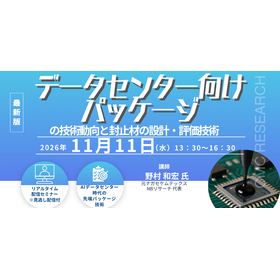
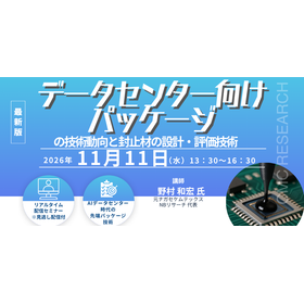
■Title: "Technological Trends in Packaging for Data Centers and Design/Evaluation Technologies for Encapsulation Materials" This presentation will explain the packaging technologies and encapsulation materials that support semiconductor devices for data centers, which continue to evolve with the spread of AI. It will organize the trends of the latest packaging technologies, such as chiplets and wafer-level packages, while systematically learning the design requirements and evaluation technologies for encapsulation materials, including high purity, moisture resistance, low stress, low dielectric loss, and high thermal conductivity. Furthermore, it will also introduce the latest trends in optoelectronic integration technologies that support next-generation data centers. - Technological trends in packaging for data centers - Design technologies for semiconductor encapsulation materials - Evaluation technologies for semiconductor encapsulation materials - Wafer-level packaging and chiplet technology - Latest trends in optoelectronic integration technology - Designers of semiconductor encapsulation materials - Engineers using semiconductor encapsulation materials - Developers of epoxy resins and hardeners - Research and development personnel from semiconductor material manufacturers
Inquire About This Product
basic information
■Event Details Date and Time: November 11, 2026 (Wednesday) 13:30 - 16:30 Participation Fee: 44,000 yen (tax included) *Includes materials and on-demand streaming *Newsletter subscribers: 39,600 yen (tax included) Instructor: Mr. Kazuhiro Nomura (Representative of NB Research) Participation Method: This seminar will be a live-streamed seminar using "Zoom." The seminar will explain the evolution of encapsulants for semiconductor packages aimed at data centers, focusing on design technology and evaluation methods. It will cover practical content including responses to low dielectric loss and high thermal conductivity, various reliability evaluation tests, and organic materials necessary for optoelectronic integration technology.
Price information
Participation Fee: 44,000 yen (tax included) *Includes materials and on-demand viewing *For our newsletter members (registration is free) 39,600 yen (tax included) ★If two or more people apply simultaneously and all applicants register as newsletter members, the participation fee per person will be half of the newsletter member price.
Delivery Time
Applications/Examples of results
- Development of semiconductor packages for AI - Design and material development of semiconductor encapsulants - Evaluation of high thermal conductivity encapsulants - Research and development of low dielectric materials - Development of devices for data centers - Development of wafer-level packages - Investigation of chiplet-related technologies - Development of materials for optoelectronic integration *Please check the related link URL for program details and application methods.
News about this product(1)
Company information

We provide the latest industrial insights to our clients. By conducting market trend analysis, publishing technology‑related books and research reports, and organizing and managing seminars, we support research and development across a wide range of industries, with a primary focus on manufacturing. Our coverage spans diverse fields such as energy, batteries, chemicals, and biotechnology.


