

Mitanis' screen masks continue to expand from IC chips to solar cells!


Achieve high productivity at low cost! Rotary screen printing machine with excellent reproducibility.


Leave the latest ultrasonic cleaning to Sonosys.


High-speed maskless aligner capable of fine drawing at 0.6μm.


We will introduce a case study that addresses the issue of "managing the aging deterioration of tension"!


Layer B has a high adhesion to the substrate, and depending on the design, it is also possible to further increase the adhesion.


Photo mask surface protection film with high durability and pattern reproducibility.


High-precision alignment (within 1μm of the target) is now possible in all directions of X-Y-Z-θx-θy-θz.


We utilize our years of expertise to manufacture a variety of industrial masks.

Single PPM for Defect Rate in Implementation - Metal Mask to Achieve a Defect Rate of 0% in Implementation

We pursue high definition and high precision masks tailored to your requests and applications, flexibly responding to quality and cost.

Samples will be displayed at the exhibition. Improved separation from printed circuit boards! Chemical resistance including organic solvents and alkali.


Shortest half-day estimate / 【Processing Example】 A5052 / Milling processing / Introduction of black anodizing! Various device parts and machined products can be ordered from just one piece!


From small size to large size, scrubbing, rinsing, and drying are all performed with one machine!

Complete removal of particles larger than 1μm and resist residue attached to the mask all at once.
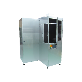
"Scrub washing + rinse" & "Hot pure water drying" two-tank simple mask cleaning device


It is possible to select an optimal acceleration based on the viscosity of the resist coating agent! We also pay attention to maintainability.


In grinding, precision management of the pad is important, but are you using a modified carrier that takes into account the type of PAD? Customizing it will also make precision management easier.


We also offer advanced repair equipment for printed circuit boards! A drying and firing control system with a minimum correction line width of 5 micrometers.

Achieve high-quality fine patterns! Introducing a photomask with excellent dimensional stability.


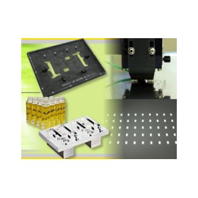
We offer a wide variety of screen masks from low mesh to high mesh! Introducing Sun Kogei's screen masks.

Excellent cost performance! There is no distortion in the design part, and the printing accuracy is outstandingly good.

Printing without blurring or jagged edges is possible! It is suitable for high-resolution color printing and thin film printing.


Mirror projection mask aligner, a unit that enables double-sided exposure with contact aligners.


Liquid hazardous materials can also be safely transported with all-fiber solutions.


We offer high-quality quartz and glass products at low prices and with short delivery times! Please feel free to consult us about anything related to quartz and glass products.


High adhesion to the substrate surface! A solder printing mask that enables excellent printing.


Utilizing photofabrication! Fine patterns can be formed!


We have a track record of supplying to major package manufacturers! We accommodate large-sized masks.

Skilled technical staff are ready to take on special requests! We can accept both EB data and GDSII.

Even without data, we can restore design data from the mask! If you are in trouble, please feel free to consult with us.

Photo masks used in various fields. We provide suitable products tailored to our customers' needs.

It's too late to ask now! What is a photomask? Here, we introduce its applications and manufacturing process! With a long history and cutting-edge technology, it achieves high reliability and high precision.


The electrode materials for special lighting by Planze are continuously evolving.


This is a photomask drawn using the latest equipment that uses a laser as the light source.


Easy setup, automatic parallel adjustment, complete non-contact gap management. Auto mask aligner with auto-alignment feature. Custom-made options available!


A mask shop that provides high-quality class photomasks "quickly," "cheaply," and "easily."

By applying finishing processes, the taper is removed, improving both appearance and dimensional accuracy!

We have a drilling machine in-house, allowing us to respond to short delivery times with integrated in-house processing!


We will provide you with the latest information on "Majesty-DI."


Mirror projection mask aligner, a unit that enables double-sided exposure with contact aligners. There is also a proven track record for IR (near-infrared) specifications.

Next-generation megasonic technology can instantly clear wafers up to 300mm.

Thorough removal of fine contaminants from wafers. High-quality cleaning achieved by Sonosys.

For precise cleaning of prisms. Sonosys ultrasonic cleaning device.

The Digital Generator is a digital control generator compatible with megasonic cleaning systems for semiconductors, electronic components, and precision instruments.


We challenge the limits of precision with high-quality natural stone, meeting the demand for accuracy in 1/1000 millimeter increments.


Test printing is possible! Printing on polyimide coverings and more can be done with high precision and fully automatically.


Machining / Firiru Co., Ltd.

Precision parts processing / stainless steel processing / SUS processed products

For those struggling with selecting positioning stages. You can find out which positioning stages are used in which processes! We will also introduce key points for selecting equipment.

Contributing to quality improvement through visual inspection and image/tension management!

We will introduce a case study that addresses the issue of "acceptance confirmation during new creation"!

We will introduce a case study that addresses the issue of "inspection after cleaning"!


High-speed semiconductor mask laser drawing device 'ULTRA'


For now, this! You can understand it in just 5 swipes! The basics of photomasks that beginners can’t ask about anymore!

<Semiconductor-related Masks - Basic Information Release> A must-see for those who are handling various masks for the first time due to departmental transfers or job changes! A detailed explanation of the structure, types, and manufacturing methods of masks.

For matters related to photo masks and materials/equipment for printed circuit boards, contact Rat Corporation.

The unique control system enables the reproducibility of patterns.

Cleanly removes stains such as crystallization! Foam-type developer cleaning agent.

Complete automation of development/etching! Ensures consistent production of high-quality products.

In response to requests from many customers, we have handled a quantity of up to 2,300 pieces.