

Compatible with 2 to 12-inch wafers. Customizable for each item.


We will provide an environment for scrub cleaning and chemical spin cleaning tests of wafers from φ2” to φ12” in response to research and development and small lot production with space-saving solutions by next spring.


High-performance, cost-effective RF/DC magnetron sputtering device for research and development.
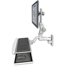

High-durability arms that can be selected according to the usage environment of medical institutions and factories, with variations and equipment integration support.


Chemical-resistant fluororubber seal! Significantly improved chemical resistance compared to conventional fluororubber.


Plasma treatment can be performed without supplying gas from the outside. It is applicable for surface treatment (pre-treatment for painting, adhesion, printing, etc.) and in the bio-medical field as well.

Speedy heating and melting!! Achieve a clean working environment!!


It is a high-precision die bonder optimized for mass production of optical devices. Additionally, we also offer the highly precise FDB210P in our lineup.

A next-generation semiconductor substrate flattening processing device that achieves both cost reduction and high quality for power semiconductor substrates! Realizing high-precision flattening processing while minimizing environmental impact.
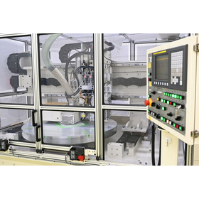
A processing technology that maximizes the performance of CMP pads, contributing to the stabilization of polishing performance and reduction of running costs through uniform surface processing!
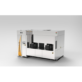

It is a device that uses a special high-pressure nozzle, allowing for cleaning and drying without the use of chemicals.


Exhibits stable high performance even with repeated long-duration door opening and closing operations! Excellent durability of the load port.


It is a low-temperature PVD coating using advanced vacuum plasma technology.


Easily have a high-output UV curing device at your fingertips. We offer three types of lamps tailored to your resin.


Possession of forklifts and ultrapure water production equipment (Organo)! Comprehensive contracting including design is also possible.

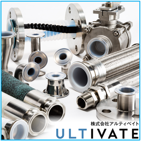
A multipurpose hybrid hose that combines the high durability of the rubber hose with the cleanliness and chemical resistance of the PFA in the fluid contact area.

A group of trade specialists! We build interactive relationships between the world and Japan.

![0_logo[1].jpg](https://image.mono.ipros.com/public/company/image/c4c/2006029/IPROS71427954949837207986.jpeg?w=280&h=280)
We perform deburring processing that meets specifications using servo press molds and laser processing.


All components are custom-made at a low cost, allowing for flexible customization. We provide one-stop service, including software support, at an attractive price.


IC Tray SUNRISE PLASTICS INDUSTRY CO., LTD (Chen Zhou Plastic)


Next-generation soldering materials that respond to modern needs with a focus on environmental compatibility and health.


A unique LED UV curing solution with numerous patents obtained! Applying UV resin curing in electronics, industry, medical, and optics!


It is a system that can be easily integrated into soldering equipment. It has good application efficiency with no waste! No splatter or bounce-back! In other words, it's gentle on both the environment and your wallet!


High-performance laser lithography equipment for research and development.


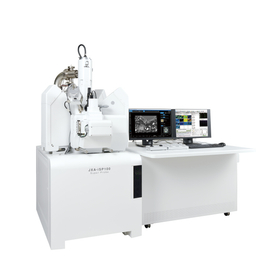
Shape observation and simple quantitative analysis using SEM-EDX.

All components are custom-made, allowing for flexible customization. We offer one-stop support, including software compatibility, at attractive prices.
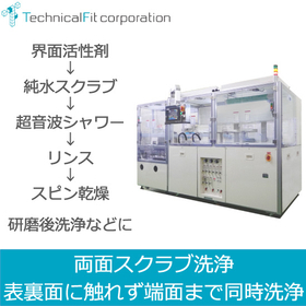
It is possible to transport, wash, and dry without touching the front and back surfaces of the work.


IPA steam cleaning and drying equipment! Achieving clean drying for devices, wafers, glass, and parts!

[No Solvent Required] Handy-type atmospheric pressure plasma device, low temperature, no charge damage! High processing performance for cleaning, surface modification, hydrophilization, and adhesion enhancement!


"Improving productivity, bond quality, and reliability" - Expanding the bonding area, equipped with advanced pattern recognition, and enhancing process control in wire bonding.


2018 edition of the NFPA-approved Japanese version materials. A sample version including up to Chapter 3 is available for free.


In addition to viewing information, data analysis is possible!


Laminating equipment compatible with a variety of films and glass.


We promptly and reliably detect and notify leaks inside equipment, piping, and water areas in data centers, semiconductor manufacturing sites, hospitals, and apartments.


Introducing semiconductor-related products such as 300mm wafer shipping containers and wafer process containers!


A fully automatic multilayer film forming device that can form multilayer films with excellent uniformity!
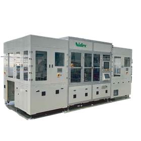

Supports a maximum of 112Kp up and down! Achieving multi-pin and high-precision inspection of large HDI boards.


Consolidating information on partnerships of semiconductor companies, such as business integrations and corporate acquisitions! Introducing information services.


By simply applying it over the equipment, approximately 10% energy-saving effect can be achieved. It can be applied without stopping the factory. We offer free energy-saving effect predictions.


Achieve high productivity at low cost! Rotary screen printing machine with excellent reproducibility.


We will perform internal wiring modifications of semiconductors aimed at circuit changes with accuracy, speed, and short delivery times.


Establishing precise cleaning equipment and a clean environment! Capable of handling aluminum, glass, ceramics, and more.


We are publishing the specifications of various grid ion sources manufactured by Kaufman & Robinson.
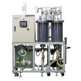

Achieving a filtration precision of 1μm! Filtration of brittle materials such as quartz glass and ceramics using a patented backwashing system! Technical documentation is also available!


A sticky sheet that can be easily removed by heating. It’s a great product that can be firmly fixed but will peel off quickly when heat is applied! Perfect for improving the manufacturing efficiency of electronic components!


Domestic ultra-compact pen-type atmospheric plasma device suitable for fine processing and laboratory applications! It can be easily used at an affordable price.


Fluororesin tubes for the semiconductor industry that shorten the cleaning process!


Seamless uniform air discharge nozzle. Length can be freely adjusted in millimeter increments.


Fluororesin coating F-200SI, effective as a corrosion prevention measure against hydrogen sulfide generated in hot spring areas, water treatment plants, livestock farming, and recycled paper factories, Rust Prevention.


Flow controller using porous metal technology (for high purity).


Compatible with high aspect ratio TGV/TSV. The world's largest chamber size (1000mm□) for ALD.

Multi-layer film formation enables the improvement of load-bearing capacity for low-temperature DLC (Diamond-like carbon) thin film hard coatings!


Numerous adoption results worldwide. We propose suitable solutions for automatic plating solution analysis in various electroplating and electroless plating processes, as well as in the Cu damascene process.


We can flexibly accommodate processing without 3D CAD data! We will do our best to meet your requests regarding tolerances and distortions, taking into account the characteristics of the material.


If you are looking to keep the relocation of the equipment cost-effective, please feel free to reach out to us.


Featuring the latest products from Tokyo Electron Kyushu, a leading company in semiconductor manufacturing equipment!


Ideal for punching seals, high-performance films, electronic components, automotive parts, and gaskets.


Value Impact Co., Ltd. offers value in "connecting." We provide tube fittings used for vacuum piping and high-pressure gas piping.


Nurturing ideas with passionate thoughts! Connecting to a further future and carving out a new tradition.

With a thermal conductivity more than 20 times that of air, it absorbs heat from heating elements! We design and manufacture heat sinks tailored to your needs based on application, shape, size, and material!


We have unique processing know-how to prevent tap breakage☆ You can trust us even with difficult-to-machine materials like Inconel!

TGV Glass Microfabrication Technology LIDE (Laser Induced Deep Etching)


Achieving insulation between the input side and the output side! It does not return leakage current from the output side device to the input.
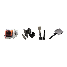

High-quality and diverse substrate transport tools.
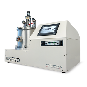
High-performance, cost-effective RF/DC magnetron sputtering system for research and development.


Dicing ring (frame) cleaning device available in two types: jet cleaning type (non-contact) and scrub cleaning type (contact).
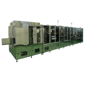
Features stable solder ball mounting and improves productivity through an inline system.
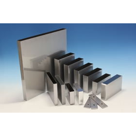

A must-see for those who find mold costs a bottleneck in battery case production! Flexible design shapes are possible with reliability equivalent to stamping processes. Numerous achievements in the aerospace industry.


Fully automatic exposure device (mask aligner) compatible with Ø2” to 6”


It is possible to perform uniform UV irradiation over the entire area of the wafer by rotating the work while irradiating.

Using conductive PP! Suitable for prototypes and small-scale transportation, shipping, and storage.


A circular rotating table made with aluminum honeycomb panels! Achieved both weight reduction and cost savings!


Significant reduction in footprint and purchase costs, increased throughput, and substantial improvement in substrate quality.


High precision, low cost, multifunctional... Comprehensive catalog of desktop wire bonders and bonding tools.

The KRI grid ion source is available in DC type and RF type.
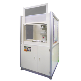
Cleaning difficult-to-clean uneven surfaces with high-pressure pulse jets! More stable cleaning results can be achieved compared to manual cleaning.


It is possible to install light and power supply together.


Just install the GEM module between the device and the host!


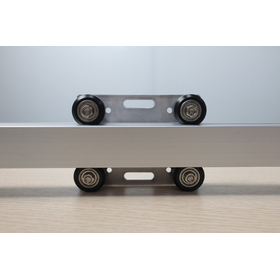
Vietnam is no longer just a cheap country.


Adopting precision ball screws enables high-accuracy positioning!
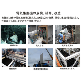

Supporting quality improvement through comprehensive maintenance of electric dust collectors.
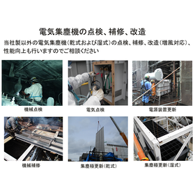
Supporting stable operation of electrical equipment through comprehensive maintenance of electric dust collectors.
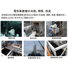
Supporting hygiene management in food factories through the maintenance of electric dust collectors.
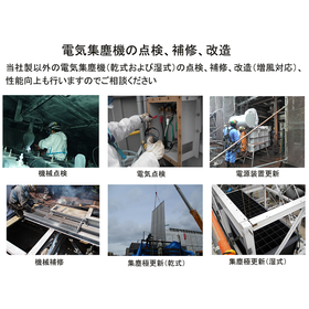
Supporting a clean environment for semiconductor manufacturing through comprehensive maintenance of electric dust collectors.