

A wide range of products including ingots and 4-inch, 6-inch, and 8-inch wafers! Leave the procurement of high-quality, low-cost SiC wafers to us.


Increased curing treatment efficiency with UV irradiation in a vacuum environment! Supports wafering up to a maximum of 8 inches! Demonstrations and customization available!


Safely and cleanly transporting wafers, the foundation of semiconductor technology!


Compact packaging of semiconductor wafers. Thin wafers can also be transported safely. Complies with ANSI/ESD S541 standards.


New CVS analysis device "894 Professional CVS" for measuring organic additives in copper sulfate plating baths and tin/lead baths.


Shape observation and simple quantitative analysis using SEM-EDX.


The AI-equipped appearance inspection device "AURCA Series" for semiconductor wafers and panels has arrived! It can also inspect semiconductor package substrates and printed circuit boards!


With a commitment to high quality and short delivery times, we will expand our business to meet the diverse needs of our customers!


It is a surface resistance value of less than 1×12Ω!


Recruiting participants for the CMC seminar to be held in Singapore on October 28, 2026!


[Sample Presentation] For metal-free applications of chemical agents in the manufacturing processes of electronic materials such as semiconductors and liquid crystals.


◆Surface roughness Ra1nm or less◆


Prevention of damage from shock and vibration!!


Fast, easy, and user-friendly! A dicing sheet applicator compatible with all standard tapes.

Partially available for free on our official website! You can view it by creating a free account.

Simultaneous measurement of inorganic and organic components in minute specific areas.


Achieves stable and high-precision micro-dispensing. The series adds TM-08S (inner diameter φ0.08), enabling further micro-dispensing.


[Factory Security] No software installation required


We will handle mass production testing (CP test / FINAL test) and test development (test programs, boards).


【Demo unit available for loan!】Wafer High-Pressure Jet Scrubber HPC-8654-H


In addition to high-purity SiC for semiconductor device components, overseas SiC wafers, and refractory SiC, we also offer contract services for laser processing that is compatible with SiC components!


Anyone can easily measure pressure and load values instantly and visualize them immediately!


Successfully conducted experiments aboard the NASA Space Shuttle!


3D implementation services (implementation services using TSV technology, etc.)

The sale of the appearance inspection device "AURCA series," which supports RDL defect inspection, bump defect inspection, and TSV defect inspection, has begun!


Due to the dry process, no water is used, making it environmentally friendly. Achieves increased productivity with zero car flows. Compared to conventional methods, it has a smaller footprint.

After cleaning on a dedicated line, it is shipped in a clean pack, making it easy to use without any hassle! A wafer transport case that also helps reduce costs!


Supports chips smaller than 0.3mm! Next-generation manufacturing equipment designed for the miniaturization of electronic components!

Achieve high productivity with high-speed pickup technology of up to 10 pcs/sec! Our unique technology ensures reliable packaging of even the smallest chips. *Customizable.


For low-cost, high-performance wet processing equipment, please leave it to us.


A rich lineup of 27 different types! We also accept custom orders, regular calibration, and repairs.

Publication of the regional distribution, production capacity, and supply-demand analysis of chip factories around the world.


Achieving excellent piezoelectric properties! We offer specifications tailored to your applications.


Numerous achievements in optical fibers and polysilicon. We conduct consistent production from metallic silicon powder.

We have a track record of supplying major semiconductor manufacturers in Japan, South Korea, and China. We provide our products with high-level foreign matter management.

It is made in Thailand with large-scale hydropower. Please consider it as a source to reduce reliance on China.

Due to domestic supply shortages! Flexible response for PEI and PAI machining from prototype to mass production with direct overseas sales. On-site measurements without drawings are also acceptable!

We provide silicon wafers optimized for individual needs!


A wafer that can easily and reliably collect microscopic foreign substances in contact with the back surface.

Leave it to us for all kinds of test pattern wafers for 3D NAND flash memory.

Numerous achievements: Various wafer processing options are available. From bare die shipment to package assembly, you can also choose the shipping method.


We offer SiC wafers at low cost starting from just one piece! Delivery time is as short as two weeks. We can provide low-priced, small quantities for the development and prototyping of power semiconductors.


Achieving reduced cycle time in chip manufacturing and high quality! Sensors for blade monitoring during wafer cutting.


Film deposition is possible on wafers ranging from 2 inches to 12 inches.

We can provide high-quality, high-purity, high-resistance FZ silicon manufactured using the FZ method with low levels of pollutants.


Bubbles-free application possible! Non-contact type for patterned surfaces can also be produced.


We propose coating equipment (spray coater) that can meet our customers' needs, utilizing years of prototype coating technology and a database.


We would like to provide information about test wafers supplied to semiconductor material manufacturers and equipment manufacturers.

Available in 200mm and 300mm! Please consult us regarding the types of films available according to your preferences.

Very useful for CMP research and development applications! Patterns with high step heights are also available.

A pattern wafer manufactured in domestic mass production, close to device grade.


Development of technologies for adhesion, control, and monitoring! Comprehensive support from design to manufacturing.


Plastic containers (Placon) that can be used in clean rooms - can be produced in small quantities.


The heating section is always a constant nozzle heater and planar heater.


Proposal for Continuous Supply Ultra-Pure Water Production System: Achieving Stable Operation 24 Hours a Day


Curing applications for wafer dicing tape, featuring stable long lifespan with UV-LED adoption.


Non-contact suspension transport of workpieces using air jets! Bernoulli chuck.

Transport ultra-thin wafers with a thickness of 20μm by bending, warping, and without damage in a non-contact manner.

It grips a micro 2.0mm IC wafer chip non-contact.
It can grasp and transfer fragile films and ultra-thin sheets non-contact.

Bernoulli chuck "Float Chuck SAC type" adopting a gas vertical jet method that reduces airflow friction loss.


<High precision, high speed, high rigidity> We offer specifications of all sizes for both atmospheric and vacuum applications!


Full cut and step cut compatible with dual spindle! Processing track record for wafer thickness of 725 to 100 μm and chip sizes of 0.5 mm or less!


Reinforcement and fixation of thin wafers are possible with electric field control that does not require adhesive!


Prototype support, small quantity support, 4 to 12 inch support, optional film thickness (10nm to 20μm), substrate arrangement possible, support for supplied substrates, short delivery time.


We provide blanket films and patterned wafers for material and device evaluation.


We accept orders for production starting from one piece, not only for modifications of existing parts and the manufacture of special tools, but also for other consumable parts.

If it is machining, it can be produced without a mold.

Our company offers products made from various materials to our customers.

Please contact us. We will search for it in our network.

Repair and reconfiguration of display devices with unknown manufacturers or maintenance providers (very welcome).


Optimal for high-temperature lead-free solder materials! Achieved mass production of gold-tin alloy plating, reducing wafer loss costs!

From prototype to mass production! We accept plating for various types of wafers!


Achieve uniform development processing with a unique spray array! Introducing a development device with excellent maintenance characteristics.


We manufacture and provide contract processing from high-purity polycrystalline silicon, which is the raw material for single crystals, to the device front-end process.


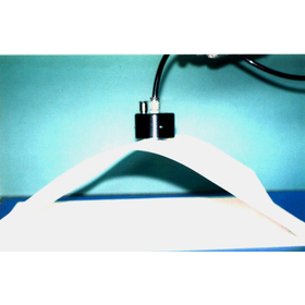
It is a device for vacuum thermal pressing into 3D shapes. It can adhere to curved surfaces, seal uneven surfaces, and follow steps.

This is a device that can contribute to reducing environmental impact.

"894 Professional CVS Analyzer" capable of multi-sample continuous automatic analysis by combining a sample changer and an electric burette.

Quantification of anions in high-concentration sodium hydroxide solution for semiconductor manufacturing using ion chromatography.

Automating quality control of the chloride ion concentration in the acidic copper plating bath used for Cu deposition on semiconductor wafers using a potentiometric automatic titration system.

Simultaneous analysis of ammonium hydroxide, hydrogen peroxide, and hydrochloric acid in the wafer cleaning tank monitored by inline near-infrared analyzer!

Process analyzer / Online analyzer for continuous monitoring of hydrogen peroxide concentration in the CMT process!

For the semiconductor industry! Process analyzer / Online analyzer for monitoring tetramethylammonium hydroxide (TMAH) in developer solutions!

Evaluation of Organic Coatings on Metals Using Electrochemical Measurement Devices Based on ISO 17463 - Paints and Varnishes

Analytical methods essential for the processes and quality control in semiconductor manufacturing.


We will obtain high-quality silicon from the market very efficiently and provide it to you!

Manufacturing of parts made of copper, brass, aluminum, and stainless steel related to electronic components and semiconductor-related components.


Flat finishing, flattening, and removal of protrusions for various flat surfaces.


Flat finishing, flattening, and removal of protrusions for various flat surfaces.