
List of Semiconductor Manufacturing Equipment products
- classification:Semiconductor Manufacturing Equipment
1036~1080 item / All 5250 items


It won't break even after 1 million repetitions! A mat switch with reliable operation, high durability, and low price. Suitable for options in machine tools as well. Please consult us about delivery t...
- Sensors


We can accommodate high resistance over 10,000 ohms, with diameters ranging from approximately 30 mm to 8 inches, and we also offer thinning and chip processing arrangements!
- Other semiconductors
- Processing Contract
- Wafer


Achieve multi-functional bonding solutions with a single unit! Specialized in bonding for batteries.


- Bonding Equipment

"Improving productivity, bond quality, and reliability" - Expanding the bonding area, equipped with advanced pattern recognition, and enhancing process control in wire bonding.


- Other processing machines
- Bonding Equipment
- Other semiconductor manufacturing equipment

The Model 1200 tabletop reflow device is an ideal tabletop unit for process development and small-scale production of microelectronics packages.


- Bonding Equipment

Supports the installation of multi-functional high-precision components! Compatible with applications requiring advanced load control and image recognition. [Demo units available for loan]


- Bonding Equipment

Stable and high-quality wire bond process management! Achieve improved operating rates and high productivity!
- Bonding Equipment
- Other mounting machines
- Other contract services

Wedge bonder equipped with a direct drive motion system and a high-performance image recognition system, achieving high productivity and reliability.


- Other processing machines
- Bonding Equipment
- Other semiconductor manufacturing equipment

Techno Alpha is the Japanese distributor of K&S wire bonders, which boasts a top-class global share in wire bonding, as well as consumables for wire bonders.


- Bonding Equipment
- Other semiconductor manufacturing equipment
- Semiconductor inspection/test equipment
![[Device Production Example] Film Fo...](https://image.mono.ipros.com/public/product/image/2063560/IPROS14926181795092471963.jpg?w=280&h=280)

From design to after-service of the equipment! We can offer various equipment proposals.
- Sputtering Equipment
![[Device Production Example] Design ...](https://image.mono.ipros.com/public/product/image/2063560/IPROS6387341858822702427.jpg?w=280&h=280)
Support for the entire lifecycle from device design to after-sales service!
- Sputtering Equipment
- Plasma surface treatment equipment
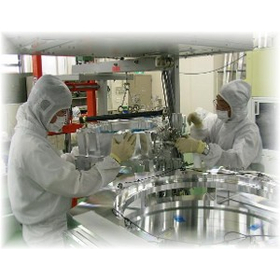
We relentlessly pursue customer satisfaction and technical expertise, contributing to society. We have extensive experience in contract manufacturing for OEMs and prototype machines.
- CVD Equipment
- Wafer processing/polishing equipment
- Other semiconductor manufacturing equipment
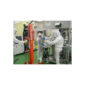
Under the management philosophy of 'pursuing customer satisfaction and technical expertise to the utmost and contributing to society,' we develop our business.
- Vacuum Equipment
- Evaporation Equipment
- Sputtering Equipment


Using conductive PP! Suitable for prototypes and small-scale transportation, shipping, and storage.
- Racks and Cases
- Other semiconductor manufacturing equipment
- cabinet


Introduced the ROKURO CEGA capable of processing at Φ0.01. Also supports simultaneous 5-axis machining.


- Ion implantation equipment


Round hole filters and honeycomb mesh, etc.! You can create freely shaped designs.


- Etching Equipment


Standard products available in a variety of sizes, customization is also OK! *Currently offering product samples to 10 people by lottery.

- Other semiconductor manufacturing equipment
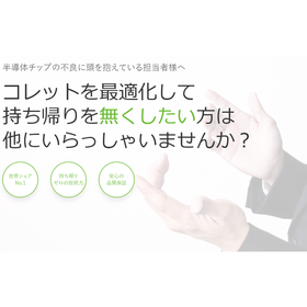
We will be exhibiting at the Kyoto Pulse Plaza, which will be held in Kyoto from February 18, 2026.
This time, Orte Corporation will exhibit at "Kyoto Pulse Plaza" again this year, following our participation in last year's semiconductor exhibition. The latest cutting-edge collets that can only be seen here will be on display! Our specialists in chip transport collets will unveil the latest lineup that solves on-site "troubles"! Be amazed by our rubber collet that achieves a contact width of less than 0.1mm! Of course, we have rubber collets that address ionizer countermeasures, as well as patented holder mechanisms that perfectly accommodate high-aspect and large chips. You will surely find yourself thinking, "This is the collet I wanted!"... We plan to showcase many actual samples! You can actually hold, touch, and experience the performance on the spot. Please come and visit our booth! We are confident that you will definitely think, "I'm glad I came to see this!" 【Exhibition Contents】 - Pickup collets (rubber/plastic/metal/others) - Bonding-related components (upward needles, dispense nozzles, transfer pins) - Wire bonding-related components (EFO torch, wire clampers, window clampers, finger clamps) - Transport components (magazine racks, IC chip trays)


Power module and secondary battery circuit formation! Digital control of position, load, and ultrasound.
- Bonding Equipment

Notice of Participation in "JPCA Show 2025" from June 4 (Wednesday) to June 6 (Friday), 2025.
Adwells Co., Ltd. will be exhibiting at the "JPCA Show 2025 (Total Solution Exhibition for Electronic Devices)" held at Tokyo Big Sight. At the exhibition, we will introduce ultrasonic application technologies such as heat sink formation, power module bonding, DMB bonding, flexible substrate bonding, and ultrasonic cutting. Additionally, we plan to display a variety of samples processed with our equipment from various fields, which we believe will be helpful in realizing new ideas and solving challenges. We invite you to visit our booth when you attend the event.


High-speed line inspection at SWIR 2K×1, 110kHz
- Monochrome camera
- Semiconductor inspection/test equipment


The micro heater can be easily wrapped around pipes and can be used even in a vacuum.
- Other semiconductor manufacturing equipment
- Food Packaging Machinery

Various shapes can be produced according to the shape of the heated object. We can manufacture even from just one piece!
- Other semiconductor manufacturing equipment
- Other processing machines


Support yield improvement through pressure management!
- Other semiconductor manufacturing equipment
- Other measurement, recording and measuring instruments

Support yield improvement through pressure management!
- Other semiconductor manufacturing equipment
- Other measurement, recording and measuring instruments
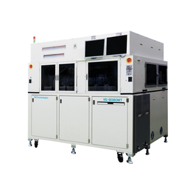

The layout and operability of the NS series remain unchanged, achieving stable low-temperature measurements.
- Tester
- Other semiconductor manufacturing equipment
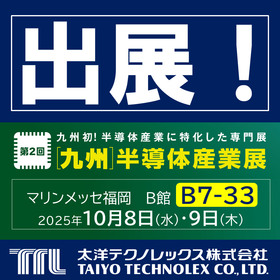

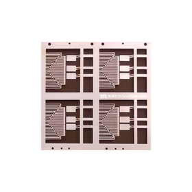
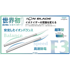
Full support from FPC design, prototyping, and mass production to board power-on testing, appearance inspection systems, and FA automation! TAIYO FPC SOLUTIONS!
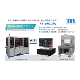
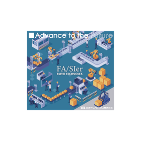
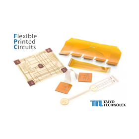
- Semiconductor inspection/test equipment
- Printed Circuit Board
- Circuit board design and manufacturing


Technological capabilities that contribute to the development and practical application of advanced materials.
- Etching Equipment
- Plating Equipment
- Other surface treatment equipment

Equipped with a function to adjust the swing angle! It can maintain an even spray balance!
- Wafer processing/polishing equipment
- Other surface treatment equipment

Design of the arrangement of transport components (rolls) developed independently by our company! Stable transport without corner bends or dents is possible.
- Etching Equipment


Utilizing hydrogen gas, stainless steel bright treatment is possible!


- stainless
- Annealing furnace
- Electric furnace


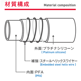
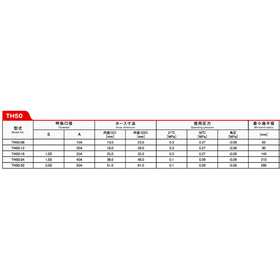
It is a top-grade fluid transfer solution that achieves visibility and flexibility.
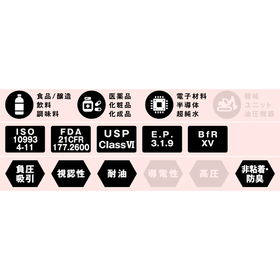
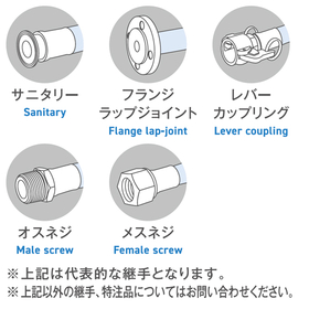
- Piping Materials
- hose
- Other semiconductor manufacturing equipment


Compact pressure gauge compatible with the gas supply system integration for semiconductors.
- Other semiconductor manufacturing equipment
- Sensors
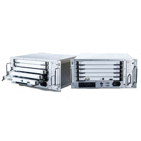
High Cost Performance Mixed Signal Tester
- Semiconductor inspection/test equipment


We respond to strict requirements for small lots! Etching processing.
- Etching Equipment

Compact yet professional! Reproducing realistic etching tests with a small amount of liquid.
- Etching Equipment

The film is transported to ensure that the load does not exceed a certain value! This achieves high spray efficiency.
- Etching Equipment

Leave silicon carbide and silicon nitride to JFC.
- Fine Ceramics
- Other machine elements
- Semiconductor inspection/test equipment

Exhibited at the 2017 High-Performance Ceramics Exhibition at Tokyo Big Sight from April 5 to 7.
Thank you to everyone who visited us. We will be exhibiting at the "High-Performance Ceramics Exhibition" held at Tokyo Big Sight in April. At our booth, we will showcase: - A new product that further enhances the fracture resistance of silicon nitride ceramics and improves thermal conductivity. - A new material that does not bend like iron, utilizing the lightweight properties of aluminum, known as "composite materials of metals and ceramics." - "Ceramic substrates" characterized by thin film and film formation technology. If you have any concerns regarding equipment design, component design, thermal design, or anything else, please feel free to stop by our booth for a consultation. We look forward to seeing you.

It is a composite material that combines the lightness of aluminum with the rigidity of steel, low thermal expansion, and excellent heat dissipation due to high thermal conductivity.
- Fine Ceramics
- Other machine elements
- Other semiconductor manufacturing equipment
Exhibited at the 2017 High-Performance Ceramics Exhibition at Tokyo Big Sight from April 5 to 7.
Thank you to everyone who visited us. We will be exhibiting at the "High-Performance Ceramics Exhibition" held at Tokyo Big Sight in April. At our booth, we will showcase: - A new product that further enhances the fracture resistance of silicon nitride ceramics and improves thermal conductivity. - A new material that does not bend like iron, utilizing the lightweight properties of aluminum, known as "composite materials of metals and ceramics." - "Ceramic substrates" characterized by thin film and film formation technology. If you have any concerns regarding equipment design, component design, thermal design, or anything else, please feel free to stop by our booth for a consultation. We look forward to seeing you.


Comparison of Grinding Methods
- Wafer processing/polishing equipment