
List of Semiconductor Manufacturing Equipment products
- classification:Semiconductor Manufacturing Equipment
1081~1125 item / All 5250 items


It won't break even after 1 million repetitions! A mat switch with reliable operation, high durability, and low price. Suitable for options in machine tools as well. Please consult us about delivery t...
- Sensors


We can accommodate high resistance over 10,000 ohms, with diameters ranging from approximately 30 mm to 8 inches, and we also offer thinning and chip processing arrangements!
- Other semiconductors
- Processing Contract
- Wafer
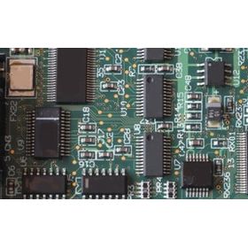


Types and Characteristics of Grinding
- Wafer processing/polishing equipment
![[Data] Plastic for Semiconductor Ma...](https://image.mono.ipros.com/public/product/image/273/2000707071/IPROS82332632158418421307.png?w=280&h=280)
Contributing to appropriate material selection! A list of plastics [chemical resistance, availability, price image] is published.
- Other semiconductor manufacturing equipment
- others

Improved wear resistance and corrosion resistance enhance equipment lifespan! It prevents the generation of particles during the production process.

- Wafer processing/polishing equipment
- Hand polishing and filing
- Other abrasives


Continuously challenging technical skills! Providing technology that can adapt to societal changes based on skills cultivated over many years.
- Other semiconductor manufacturing equipment


Changing the common sense of testing. AMB5600, an innovative platform that supports diverse ICs.
- Tester
- Testing Equipment and Devices

Supports up to 4096 channels, a multi-site open short tester that achieves the fastest test time in the industry.
- Tester
- Testing Equipment and Devices


IC Tray SUNRISE PLASTICS INDUSTRY CO., LTD (Chen Zhou Plastic)
- Other semiconductor manufacturing equipment


Achieving semi-automation with a work transport device! The transport device allows for flexible settings.
- Other semiconductor manufacturing equipment

Each tray can hold up to 100 sheets! High-precision cutting and checking functions condensed into a compact body.
- Other semiconductor manufacturing equipment

High-end model: A handler that thoroughly pursues excellent stability and significant reduction in working hours.
- Semiconductor inspection/test equipment
- Tester

High-end model: A handler that thoroughly pursues excellent stability and significant reduction in working hours.
- Tester
- Circuit Board Inspection Equipment

Middle Range Model: A handler that thoroughly pursues excellent stability and significant reduction in work time.
- Tester
- Circuit Board Inspection Equipment

Middle-range model: A handler that thoroughly pursues excellent stability and significant reduction in working time.
- Tester
- Circuit Board Inspection Equipment


Leave aluminum processing to us! 【Aluminum cutting processing, prototyping, development, design, custom-made, mass production, Osaka】

- valve
- Other semiconductor manufacturing equipment
![[Demo video available] Imitation po...](https://image.mono.ipros.com/public/product/image/155/2001501180/IPROS07783704546326619705.jpeg?w=280&h=280)

No specialized robot teaching program is needed! Just give simple instructions, and polishing can be done.
- Wafer processing/polishing equipment
![[Production Example] Self-Checkout](https://image.mono.ipros.com/public/product/image/2093823/IPROS4502456482090299908.jpg?w=280&h=280)

Integrated production of LOT200! A case where we were able to meet delivery deadlines with the cooperation of our suppliers.
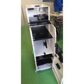
- Resist Device
- register


Low elasticity makes bending of FPC easy. Contributes to thinner, lighter designs and increased design flexibility.
- Resist Device


We solve your problems with our years of cultivated skilled processing techniques and the latest equipment! We can accommodate a wide range of needs, from various precision parts processing to large-s...
- Other industrial robots
- Other Auto Parts
- Other semiconductor manufacturing equipment
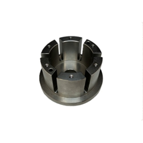
[Web Page Publication] Lathe Processing and Complex Lathe Processing
【Scope of Response and System】 - Supported Parts: Round components such as shafts, flanges, rollers, etc. - Supported Lots: From a single prototype to mass production - Processing Details: Turning and milling processing using a composite lathe. Wire electrical discharge machining, shape electrical discharge machining, heat treatment, and surface treatment can be combined as needed. - Integrated Response: One-stop service from material procurement to cutting processing, heat treatment, surface treatment, inspection, and shipping (single point of contact). - Response Speed: Initial response in as little as 60 minutes / formal quotation in as little as 2 business days. - Delivery Time: Shipping in as little as 6 business days after order. - Individual Consideration: For difficult-to-cut materials, complex shapes, and non-standard sizes, feasibility will be individually considered based on the drawings.


It is a device that aligns the orientation of the notches and orientation flats of wafers stored in a designated cassette.
- Other semiconductor manufacturing equipment
- Other industrial robots

From site surveys to design and construction, experienced engineers will handle it!
- Other electronic parts
- Sputtering Equipment


Designed a high-efficiency dryer using near-infrared halogen lamps! By promoting drying and effects from the inside, it reduces un-dried and un-cured areas! Energy-saving and long-lasting!


- Other semiconductor manufacturing equipment

Near Infrared Dryer Promo Series
Customize the "Near Infrared Dryer Promo" to fit your purpose and size! The "Promo Series" includes: - Paint dryers - Dryers for inkjet printers Both can be customized to fit your factory layout, purpose, environment, and desired performance!! - Existing dryers lack power... - They don't fit the size of conveyors... - There is nothing that can be used in the available space... etc... We can create an original design tailored to your needs. Please feel free to consult with us. You can check the basic specifications on our website.


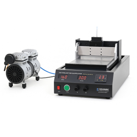


Contributing to the reduction of chemical usage and the lowering of wastewater treatment loads! A wide lineup of functional water devices.
- Other semiconductor manufacturing equipment
- Other cleaning machines

Advanced electrical resistivity control technology suppresses static electricity in ultra-pure water!!
- Other semiconductor manufacturing equipment

Full package of RO + EDI! Environmentally friendly pure water system (pure water production system)
- Other semiconductor manufacturing equipment
- others

Easily in places where pure water is needed!
- Other semiconductor manufacturing equipment


A film deposition platform for semiconductor wafers and advanced packaging capable of various film deposition treatments.
- Sputtering Equipment
- Etching Equipment
- CVD Equipment

Providing mass production solutions for high-speed and flexible substrate film deposition applications!
- Sputtering Equipment
- Etching Equipment


The illumination distribution of the exposure light source is within ±5%! A lineup of desktop and standalone models is available.
- Wafer processing/polishing equipment

We offer sizes of 4 inches and 8 inches! It has high versatility compatible with round and square samples.
- Other semiconductor manufacturing equipment


Simultaneous processing of stainless materials such as SUS316 using CNC lathes and machining centers. Manufacturing high-precision ring parts for semiconductor production.
- Other semiconductor manufacturing equipment
- Processing Contract

Flagship model: A handler that thoroughly pursues excellent stability and significant reductions in working time.
- Semiconductor inspection/test equipment
- Circuit Board Inspection Equipment
- Testing Equipment and Devices


Meeting the high cleanliness standards required in the semiconductor and medical device fields. We carry out everything from precision cleaning to packaging and assembly in a consistent clean environm...
- CVD Equipment
- Sputtering Equipment
- Resist Device

Pre-treatment for metal structure inspection will be carried out due to surface corrosion caused by chemicals.
- Other services
- Processing Contract
- Etching Equipment
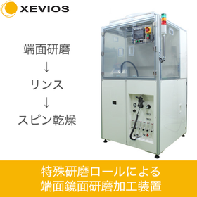

Polishing equipment (Edge Polish) that performs mirror polishing, rough polishing, and cleaning using filtered water and pure water as the medium without slurry.
- Other semiconductor manufacturing equipment

Flexibility, compact design, and low investment costs! An ideal choice for small-scale production.
- Sputtering Equipment
- Etching Equipment
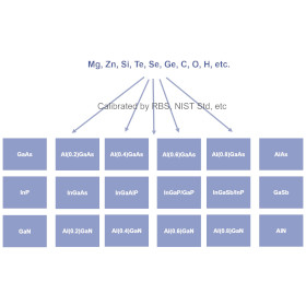

Correction of sensitivity coefficients and sputtering rates across all depths in response to changes in the sample matrix, enabling high-precision depth profile analysis.
- Contract Analysis
- Secondary ion mass spectrometer
- Ion implantation equipment
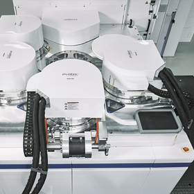
Extremely low Rc system design in the industry and the highest level of inter-wafer reproducibility!
- Sputtering Equipment
- Etching Equipment
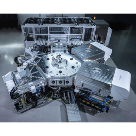
Higher productivity for PLP! More process possibilities. Optimized for advanced packaging.
- Sputtering Equipment
- Etching Equipment
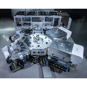
Evatec officially enters the next-generation packaging market in Japan with CLUSTERLINE 600 - Expanding business development towards the era of Panel-Level Packaging for AI and HPC.
Evatec AG (headquartered in Switzerland) is intensifying the deployment of its large panel-compatible coating platform "CLUSTERLINE 600" in the Japanese market and will fully enter the rapidly growing next-generation packaging market for AI (artificial intelligence) and high-performance computing (HPC). In the global semiconductor ecosystem, the transition to new manufacturing architectures such as large interposers, ultra-high-density RDL (Redistribution Layer), glass core substrates, and panel-level packaging is accelerating. In particular, with the increasing size of AI packages, the shift from traditional 300mm wafer-based manufacturing to 600mm class panel processes is gaining attention as a next-generation manufacturing technology. Evatec positions this change as one of the most important growth opportunities in the semiconductor industry over the next decade. By making the CLUSTERLINE 600 its core product, the company aims to expand its advanced packaging business in the Japanese market and support customers' technology development and mass production in areas such as panel-level packaging, advanced IC substrates, and glass core substrates.
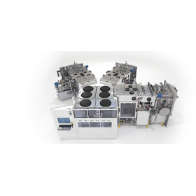
Introducing the BAK deposition platform that allows for various chamber sizes and process automation options.
- Evaporation Equipment


A unique LED UV curing solution with numerous patents obtained! Applying UV resin curing in electronics, industry, medical, and optics!
- Other semiconductor manufacturing equipment
- LED Module
- Ultraviolet irradiation equipment
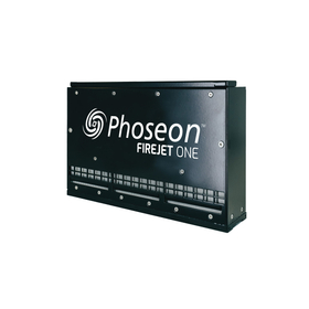
Expanding UV LED products to strengthen response to the growing and diversifying needs for ultraviolet curing.
Excelsius Noble Light Japan Co., Ltd. (Headquarters: Bunkyo-ku, Tokyo, President: Masahiko Suzuki, hereinafter referred to as "the Company") will expand its product portfolio of UV LEDs, one of the light sources for UV curing, and strengthen the provision of UV curing process solutions in new growth areas. In January 2024, the Company was absorbed by Excelsius Technologies, headquartered in the United States (hereinafter referred to as "Excelsius"), and is now handling UV LED products previously managed by its predecessor, Heraeus Noblelight Japan Co., Ltd., and Foseon Technology Japan Co., Ltd., as well as Excelsius. These products encompass a wide range of UV LED light sources for line and area irradiation as well as spot irradiation, regardless of cooling methods. As market demands become increasingly diverse, the Company has established a system that enables more detailed proposals to a broad range of industries through this product expansion.