
List of Semiconductor Manufacturing Equipment products
- classification:Semiconductor Manufacturing Equipment
4141~4185 item / All 5250 items


It won't break even after 1 million repetitions! A mat switch with reliable operation, high durability, and low price. Suitable for options in machine tools as well. Please consult us about delivery t...
- Sensors


We can accommodate high resistance over 10,000 ohms, with diameters ranging from approximately 30 mm to 8 inches, and we also offer thinning and chip processing arrangements!
- Other semiconductors
- Processing Contract
- Wafer


Due to the low height of the scale, it can be installed directly on the existing foundation, making it easy to load and unload the measured items (no foundation work required) from 19mm onward.
- Other process controls
- Other semiconductor manufacturing equipment

The platform scale load cell with excellent load-bearing capacity is ideal for measuring large containers due to its caster-equipped frame.
- Weight related measuring instruments
- Scale
- Other semiconductor manufacturing equipment


Integration of processing into a unified device! A laser system that improves production efficiency through automatic cutting.
- Circuit board processing machine
- Touch Panel
- Etching Equipment

High efficiency through high-speed processing! Laser system equipped with LD-excited solid UV laser.
- Wafer processing/polishing equipment
- Other semiconductor manufacturing equipment


It is a high-voltage power supply for TFE electron guns!
- Semiconductor inspection/test equipment
- Electron beam lithography equipment
- Other processing machines

TFE electron gun, high-voltage power supply device "FE503XP" for electron beam lithography!
- Semiconductor inspection/test equipment
- Electron beam lithography equipment
- Other processing machines

This is the high-voltage power supply unit 'IB303XS' for FIB ion guns, which also helps shorten the development period!
- Semiconductor inspection/test equipment
- Electron beam lithography equipment
- Other processing machines

This is the "IB303XP," a high-voltage power supply for FIB ion guns that also helps shorten the development period!
- Semiconductor inspection/test equipment
- Electron beam lithography equipment
- Other processing machines

This is the drive power supply 'XE303XP' exclusively for soft X-ray tubes using a thermal FE emitter!
- Semiconductor inspection/test equipment
- Electron beam lithography equipment
- Other processing machines

It is a high-precision high-voltage power supply device for TFE electron guns!
- Semiconductor inspection/test equipment
- Electron beam lithography equipment
- Other processing machines

It is the high-voltage power supply unit "FE103XP" for CD-SEM and review SEM!
- Semiconductor inspection/test equipment
- Electron beam lithography equipment
- Other processing machines


We mainly handle the total coordination from plating materials to equipment.
- Other semiconductor manufacturing equipment
- Other clean room equipment and facilities


Vacuum-Compatible Micro Linear Actuator <MLA>
- Other semiconductor manufacturing equipment
- Other physicochemical equipment
- Analytical Equipment and Devices

Hermetic feedthrough
- Electron beam lithography equipment
- Other semiconductor manufacturing equipment
- Analytical Equipment and Devices

Vacuum Non-Magnetic USM Drive Unit <Custom>
- Electron beam lithography equipment
- Other semiconductor manufacturing equipment
- Analytical Equipment and Devices

Vacuum-compatible positioning table <VT>
- Other semiconductor manufacturing equipment
- Other physicochemical equipment
- Analytical Equipment and Devices

Vacuum-compatible positioning table <MT>
- Other semiconductor manufacturing equipment
- Other physicochemical equipment
- Analytical Equipment and Devices

Vacuum-compatible positioning table <PT>
- Other semiconductor manufacturing equipment
- Other physicochemical equipment
- Analytical Equipment and Devices


Energy-saving environment and safety system engineering in a wide range of fields handled by trading companies!
- CVD Equipment
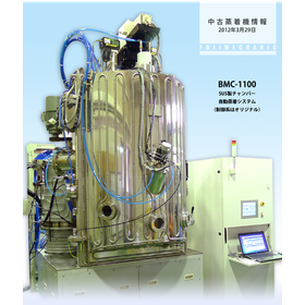

We provide vacuum deposition equipment and related maintenance services.
- Evaporation Equipment
- CVD Equipment
- Sputtering Equipment


Achieving high-precision inspection! Fully compatible with appearance inspection of chip components from fine chips to special sizes.
- Semiconductor inspection/test equipment
- Inspection robot


A latest universal gang programmer that supports writing from 1 to 64 pieces.
- Other semiconductor manufacturing equipment


A jacket roll that achieves a temperature distribution within ±0.5℃ at a roll surface temperature of 250℃.
- Heating device
- Coater
- Food Packaging Machinery

Notice of participation in the 9th Advanced Functional Film Exhibition from December 5 (Wednesday) to December 7 (Friday), 2018.
Tokuden Co., Ltd. will exhibit at the 9th High-Performance Film Exhibition held from December 5 (Wednesday) to December 7 (Friday), 2018. High-performance films are functional films that are active in various fields such as electronics, automobiles, building materials, pharmaceuticals, and food packaging. This exhibition showcases everything from these films to molding processing technologies in the film industry. Our company has a basic management stance of producing a small variety of products on order and possesses the capability to carry out consistent production activities from product design planning. At this exhibition, we will showcase air-cooled hybrid rolls and induction heating jacket rolls. <Booth Number> ■ Hall 4 E763 *If you would like a complimentary invitation ticket, please contact us through the inquiry form.


Rubycell is a new material that can replace fabric, resin sheets, and leather, offering unique applications such as in fashion components.
- Organic Natural Materials
- Other cleaning tools
- CMP Equipment


Grinding device, etching line
- Other processing machines
- Wafer processing/polishing equipment

Emulsion glass, processing of chrome masks.
- Photomask


Achieving a flatness accuracy of 0.001mm or less (for φ12 inches).
- Semiconductor inspection/test equipment
- Wafer processing/polishing equipment
- Processing Jig
The second installment of the TDC introduction video has been completed!
The introduction video part 2 of TDC has been completed. This time, it features an introduction to management by our president, Akabane. It's a short movie of about one minute, so please take a look. You can watch the video from the "Related Information" section below. Title: TDC Management Now, we are exhibiting at "Nanotech 2018," which is being held at Tokyo Big Sight starting today. We are showcasing not only mirror samples of various materials but also finely crafted precision parts and inner diameter mirror products created through lap polishing. Additionally, we have mirror plates of size 400 and large rolls of about one meter, so please take this opportunity to check them out. Since today is Valentine's Day, we will be providing coffee and chocolate for three days. Feel free to stop by. <Exhibitors> 2/14 (Wed): President, Fujino, Arisa 2/15 (Thu): President, Fujino, Maeda 2/16 (Fri): President, Fujino, Arisa, Maeda ★ Technical meetings are also possible ★ All of our staff are looking forward to your visit.

It can be used in various fields, and blast polishing of resin plates is also possible.
- others
- Wafer processing/polishing equipment


It is a positioning support unit that allows for precise positioning of workpieces and other items at each stage of the manufacturing process quickly and simply.

- Conveyor
- Semiconductor inspection/test equipment
- Wafer processing/polishing equipment


Quality born from abundant achievements and management. We will continue to meet expectations across a wide range of fields!
- Other semiconductor manufacturing equipment
- others
- Processing Contract


A tabletop vacuum plasma device that can introduce various gases such as air, oxygen, nitrogen, and argon! It can be used for surface modification and cleaning of materials♪
- Other semiconductor manufacturing equipment

Plasma treatment can be performed without supplying gas from the outside. It is applicable for surface treatment (pre-treatment for painting, adhesion, printing, etc.) and in the bio-medical field as ...
- Other semiconductor manufacturing equipment

We have started selling a gas-free atmospheric pressure plasma device.
Plasma treatment can be performed without supplying gas from the outside. It can also be used in surface treatment (pre-treatment for painting, adhesion, printing, etc.) and in the fields of bio and dental medicine. By eliminating the need for gas, we have reduced gas costs and impacts on the human body.

Domestic ultra-compact pen-type atmospheric plasma device suitable for fine processing and laboratory applications! It can be easily used at an affordable price.
- Other semiconductor manufacturing equipment
- Bonding Equipment
- Circuit board processing machine

NEW! "Rotating Plasma Device"! Exhibiting at the International Frontier Industry Messe 2012 in Kobe from September 6 to 7. ■ Demo units available at the exhibition booth. Popular for surface modification and cleaning applications.
New Product! Rotating Plasma Device Debuts at Trade Show! 【Trade Show Name】International Frontier Industry Messe 2012 【Dates】 September 6 (Thursday) - 7 (Friday), 2012 10:00 - 17:00 【Venue】Kobe International Exhibition Hall, Building 2 (Kobe Port Island) 【Expected Exhibition Scale】 200 booths (including concurrently held events) * FY 2011 results: 239 companies, 271 booths 【Expected Number of Visitors】 15,000 people * FY 2011 results: 17,253 people 【Booth】 Booth Number B-07 Displayed at the booth of 'Kyoto Environmental Nanocluster (Kyoto Institute of Advanced Technology)' 【Presentation】 September 7 (Friday) Presentation Corner A 11:00-11:20 【Exhibition Content】 ☆ Live Demonstration Tabletop Vacuum Plasma Device YHS-R Rotating Vacuum Plasma Device YHS-DOS ■ Sakigake Semiconductor Special Exhibition Page http://www.sakigake-semicon.co.jp/international-industrial-fair2012_plasma.html

[Domestic] Low temperature, no charge damage! Simple atmospheric pressure plasma device with high processing performance for cleaning, surface modification, hydrophilization, and adhesion enhancement!...
- Other semiconductor manufacturing equipment

[No Solvent Required] Handy-type atmospheric pressure plasma device, low temperature, no charge damage! High processing performance for cleaning, surface modification, hydrophilization, and adhesion e...
- Other semiconductor manufacturing equipment
- Bonding Equipment
- Circuit board processing machine
NEW! "Rotating Plasma Device"! Exhibiting at the International Frontier Industry Messe 2012 in Kobe from September 6 to 7. ■ Demo units available at the exhibition booth. Popular for surface modification and cleaning applications.
New Product! Rotating Plasma Device Debuts at Trade Show! 【Trade Show Name】International Frontier Industry Messe 2012 【Dates】 September 6 (Thursday) - 7 (Friday), 2012 10:00 - 17:00 【Venue】Kobe International Exhibition Hall, Building 2 (Kobe Port Island) 【Expected Exhibition Scale】 200 booths (including concurrently held events) * FY 2011 results: 239 companies, 271 booths 【Expected Number of Visitors】 15,000 people * FY 2011 results: 17,253 people 【Booth】 Booth Number B-07 Displayed at the booth of 'Kyoto Environmental Nanocluster (Kyoto Institute of Advanced Technology)' 【Presentation】 September 7 (Friday) Presentation Corner A 11:00-11:20 【Exhibition Content】 ☆ Live Demonstration Tabletop Vacuum Plasma Device YHS-R Rotating Vacuum Plasma Device YHS-DOS ■ Sakigake Semiconductor Special Exhibition Page http://www.sakigake-semicon.co.jp/international-industrial-fair2012_plasma.html

Dry film for thin material compatibility, PSR peeling device.
- Other semiconductor manufacturing equipment

The unique control system enables the reproducibility of patterns.
- Photomask


No need for waste liquid treatment! Thorough removal of particles and oil with ultra-fine dry ice powder.
- Other cleaning machines
- Other semiconductor manufacturing equipment
- Other optical parts

High-end mechanical stage with 6D quality.
- Other physicochemical equipment
- Distance measuring device
- Stepper


Heating element for semiconductors
- Other heaters
- Electric furnace
- Oxidation/Diffusion Device

Cylinder type heater (cylindrical)
- Other heaters
- Electric furnace
- Oxidation/Diffusion Device

Heater module for manufacturing a single wafer in the electronics and semiconductor industry!
- Other heaters
- CVD Equipment
- Annealing furnace

Super Tarl HT (high-temperature semi-cylindrical type, maximum furnace temperature 1675°C)
- Other heaters
- Electric furnace
- Annealing furnace

Super Tarl Half Cylinder Type
- Other heaters
- Electric furnace
- Annealing furnace