
List of Semiconductor inspection/test equipment products
- classification:Semiconductor inspection/test equipment
1~15 item / All 750 items


It won't break even after 1 million repetitions! A mat switch with reliable operation, high durability, and low price. Suitable for options in machine tools as well. Please consult us about delivery t...
- Sensors


We can accommodate high resistance over 10,000 ohms, with diameters ranging from approximately 30 mm to 8 inches, and we also offer thinning and chip processing arrangements!
- Other semiconductors
- Processing Contract
- Wafer

Please use it for demonstration tests and research and development.
- Processing Contract
- Contract manufacturing
- Semiconductor inspection/test equipment


Visualize surface foreign substances, dirt, and scratches! It is well-received as a daily management tool for yield management, quality control, cleaning management, and hygiene management. *Demo unit...
- Visual Inspection Equipment
- Semiconductor inspection/test equipment
- Defect Inspection Equipment
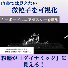
17th High-Performance Materials WEEK [Tokyo] We will be exhibiting a fine particle visualization system at the 17th High-Performance Film Exhibition. (September 30, 2026 (Wed) - October 2, 2026 (Fri) / Makuhari Messe, Hall 2)
The particle visualization technology developed under our brand "ViEST" has a very high level of detection sensitivity that allows for real-time visualization of the suspended and adhered states of micro and nano-sized particles. We are expanding our sales of visualization systems and providing evaluation services (such as investigating particles and airflow in production processes, manufacturing equipment, and factory environments, evaluating the performance of cleaning products, and proposing yield improvement measures) both domestically and internationally. We consistently support the identification of causes and the formulation of countermeasures by visualizing fine foreign substances, particle adhesion due to static electricity, and variations in cleanliness that are problematic in the film manufacturing process. The following are some examples of applications, but by utilizing our technology, we can strongly promote the resolution of various issues such as the deterioration of defect rates caused by fine foreign substances, visualization of clean airflow, and concerns regarding site cleanliness. - Visualization of foreign matter contamination and adhesion mechanisms in the coating and drying processes - Visualization of dust generation and re-adhesion during roll transportation and consideration of countermeasures - Evaluation of airflow and cleanliness within clean booths/clean rooms - Identification of dust sources within manufacturing equipment and promotion of cleanliness - Reduction of foreign matter adhesion risk on film surfaces and improvement of yield

It excels in high sensitivity detection, quantification, and portability, making it suitable for quality inspection and research and development settings. It contributes to the detection of minute for...
- Semiconductor inspection/test equipment
- Other Sanitation Inspections
- Other appearance and image inspection equipment
17th High-Performance Materials WEEK [Tokyo] We will be exhibiting a fine particle visualization system at the 17th High-Performance Film Exhibition. (September 30, 2026 (Wed) - October 2, 2026 (Fri) / Makuhari Messe, Hall 2)
The particle visualization technology developed under our brand "ViEST" has a very high level of detection sensitivity that allows for real-time visualization of the suspended and adhered states of micro and nano-sized particles. We are expanding our sales of visualization systems and providing evaluation services (such as investigating particles and airflow in production processes, manufacturing equipment, and factory environments, evaluating the performance of cleaning products, and proposing yield improvement measures) both domestically and internationally. We consistently support the identification of causes and the formulation of countermeasures by visualizing fine foreign substances, particle adhesion due to static electricity, and variations in cleanliness that are problematic in the film manufacturing process. The following are some examples of applications, but by utilizing our technology, we can strongly promote the resolution of various issues such as the deterioration of defect rates caused by fine foreign substances, visualization of clean airflow, and concerns regarding site cleanliness. - Visualization of foreign matter contamination and adhesion mechanisms in the coating and drying processes - Visualization of dust generation and re-adhesion during roll transportation and consideration of countermeasures - Evaluation of airflow and cleanliness within clean booths/clean rooms - Identification of dust sources within manufacturing equipment and promotion of cleanliness - Reduction of foreign matter adhesion risk on film surfaces and improvement of yield


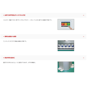
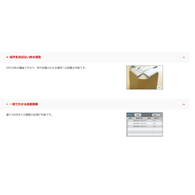
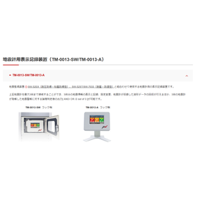
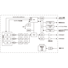
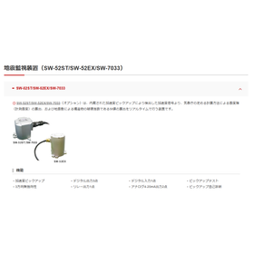
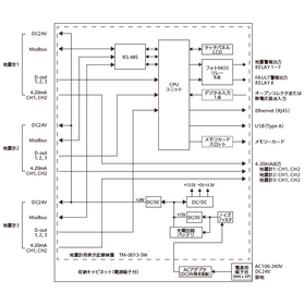
Up to 3 earthquake monitoring devices can be connected.
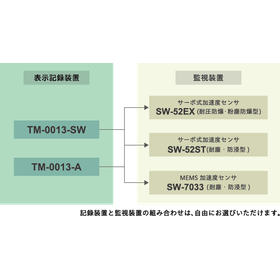
- Other machine tools
- Semiconductor inspection/test equipment
- Metal bearings
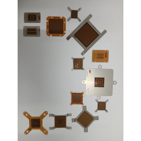

A sheet socket that enables stable inspection in semiconductor back-end process inspection! What is "PCR" that allows for high-speed and high-density measurements? Technical materials on operating pri...
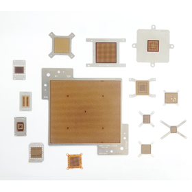
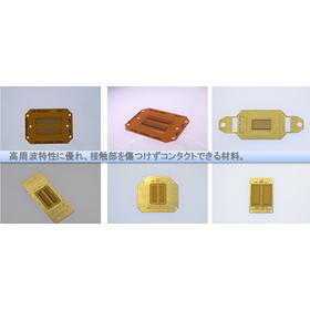
- Other electronic parts
- socket
- Semiconductor inspection/test equipment
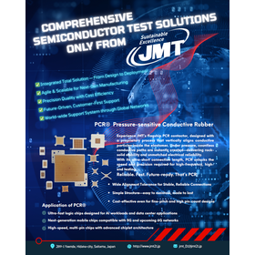
Test solution that does not damage solder balls or measurement substrates with soft contact!
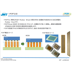
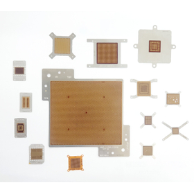
- Semiconductor inspection/test equipment
- Printed Circuit Board

An electrical characteristic testing system that maximizes the performance of power devices for EV control.
- Tester
- Semiconductor inspection/test equipment
- Testing Equipment and Devices