List of Other semiconductors products

  • classification:Other semiconductors

406~420 item / All 2678 items

Displayed results

It won't break even after 1 million repetitions! A mat switch with reliable operation, high durability, and low price. Suitable for options in machine tools as well. Please consult us about delivery t...

  • Sensors

Added to bookmarks

Bookmarks list

Bookmark has been removed

Bookmarks list

You can't add any more bookmarks

By registering as a member, you can increase the number of bookmarks you can save and organize them with labels.

Free membership registration

We can accommodate high resistance over 10,000 ohms, with diameters ranging from approximately 30 mm to 8 inches, and we also offer thinning and chip processing arrangements!

  • Other semiconductors
  • Processing Contract
  • Wafer

Added to bookmarks

Bookmarks list

Bookmark has been removed

Bookmarks list

You can't add any more bookmarks

By registering as a member, you can increase the number of bookmarks you can save and organize them with labels.

Free membership registration

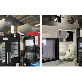
From semiconductor and LCD manufacturing equipment parts to nursing and welfare equipment parts. MINWA delivers high-precision and high-quality machining.

  • Other semiconductors
  • LCD display
  • Other machine elements

Added to bookmarks

Bookmarks list

Bookmark has been removed

Bookmarks list

You can't add any more bookmarks

By registering as a member, you can increase the number of bookmarks you can save and organize them with labels.

Free membership registration

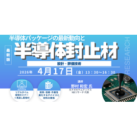
The encapsulating materials for advanced semiconductor packages require various characteristics such as low stress, moisture resistance, and high reliability. Guidelines for the design and evaluation ...

  • Other semiconductors
  • Engineering Plastics
  • Technical Seminar

Added to bookmarks

Bookmarks list

Bookmark has been removed

Bookmarks list

You can't add any more bookmarks

By registering as a member, you can increase the number of bookmarks you can save and organize them with labels.

Free membership registration

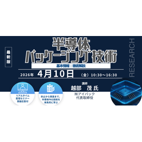
A systematic explanation from the basics of semiconductor packaging to the design and evaluation of encapsulation materials. Leading experts thoroughly organize practical perspectives from WLP/PLP to ...

  • Other semiconductor manufacturing equipment
  • Other semiconductors
  • Technical Seminar

Added to bookmarks

Bookmarks list

Bookmark has been removed

Bookmarks list

You can't add any more bookmarks

By registering as a member, you can increase the number of bookmarks you can save and organize them with labels.

Free membership registration

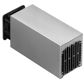
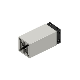
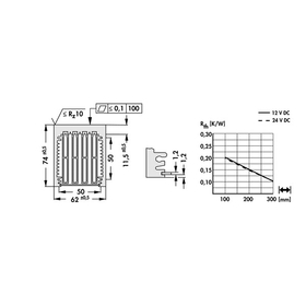
For thermal management of medium-sized devices. You can specify the ideal length in 1mm increments, without being constrained by the fixed sizes in the catalog, to match the enclosure space.
  • la6.eps.jpg
  • csm_1zeilMag_weiss_E_b78887b03c.jpg
  • Other semiconductors

Added to bookmarks

Bookmarks list

Bookmark has been removed

Bookmarks list

You can't add any more bookmarks

By registering as a member, you can increase the number of bookmarks you can save and organize them with labels.

Free membership registration

Not constrained by fixed catalog sizes. You can specify the ideal length in millimeters to match thermal design and enclosure space. Additional processing can also be handled in bulk!
  • csm_1zeilMag_weiss_E_b78887b03c.jpg
  • Other semiconductors

Added to bookmarks

Bookmarks list

Bookmark has been removed

Bookmarks list

You can't add any more bookmarks

By registering as a member, you can increase the number of bookmarks you can save and organize them with labels.

Free membership registration

Pin fin heat sink, width 40mm, height 20mm, length 40mm, material: Al99.5.

  • ick_s40x40x20.eps.jpg
  • csm_1zeilMag_weiss_E_b78887b03c.jpg
  • Other semiconductors

Added to bookmarks

Bookmarks list

Bookmark has been removed

Bookmarks list

You can't add any more bookmarks

By registering as a member, you can increase the number of bookmarks you can save and organize them with labels.

Free membership registration

Square pin fin heat sink, width 50mm, height 25mm, length 50mm, material: Al99.5.

  • ick_s50x50x25.eps.jpg
  • csm_1zeilMag_weiss_E_b78887b03c.jpg
  • Other semiconductors

Added to bookmarks

Bookmarks list

Bookmark has been removed

Bookmarks list

You can't add any more bookmarks

By registering as a member, you can increase the number of bookmarks you can save and organize them with labels.

Free membership registration

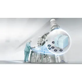
Custom formulations for important applications

  • Other semiconductors
  • Other medical supplies and cosmetic manufacturing materials
Added to bookmarks

Bookmarks list

Bookmark has been removed

Bookmarks list

You can't add any more bookmarks

By registering as a member, you can increase the number of bookmarks you can save and organize them with labels.

Free membership registration

Added to bookmarks

Bookmarks list

Bookmark has been removed

Bookmarks list

You can't add any more bookmarks

By registering as a member, you can increase the number of bookmarks you can save and organize them with labels.

Free membership registration

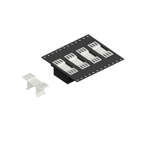
For heat dissipation of surface mount packages such as DPAK, D2PAK, and SO-8. Our compact design reliably solves thermal issues in power converters and power supply boards.
  • 1745191615.jpg
  • csm_1zeilMag_weiss_E_b78887b03c.jpg
  • Other semiconductors

Added to bookmarks

Bookmarks list

Bookmark has been removed

Bookmarks list

You can't add any more bookmarks

By registering as a member, you can increase the number of bookmarks you can save and organize them with labels.

Free membership registration

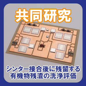
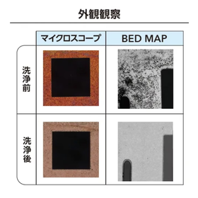
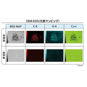
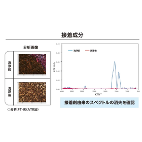
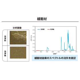
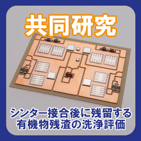
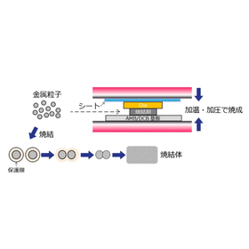
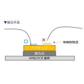
We conducted a cleaning evaluation using samples created under conditions that are likely to leave residues intentionally!
  • シンター接合後に2.png
  • シンター接合後に3.png
  • シンター接合後に4.png
  • シンター接合後に5.png
  • シンター接合後に6.png
  • シンター接合後に7.png
  • シンター接合後に8.png
  • Other semiconductors

Added to bookmarks

Bookmarks list

Bookmark has been removed

Bookmarks list

You can't add any more bookmarks

By registering as a member, you can increase the number of bookmarks you can save and organize them with labels.

Free membership registration
シンター接合後に残留する有機物残渣の洗浄評価.png

A page on "Cleaning evaluation of organic residue remaining after sintering" has been added.

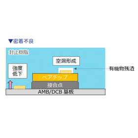
In the field of power semiconductors for automotive and industrial applications, the adoption of "sintering bonding" as a joining technology that achieves high resistance and high reliability against thermal stress is expanding, replacing solder bonding. Similar to no-clean solder bonding technology, sintering bonding is fundamentally designed to be "no-clean." However, the currently mainstream sintering bonding methods are conducted under high temperature and high pressure conditions, which can lead to the generation and adhesion of residues during the bonding process, potentially affecting subsequent processes and long-term reliability. Cleaning is one proposed solution to this issue. Although there is a "no-pressure" method for sintering bonding, its applications tend to be limited from the perspective of strength and reproducibility. Additionally, while it is residue-free, it is not "zero residue," so cleaning can also be a viable solution for achieving reliability. Detailed content of the technical column can be viewed through the related link.
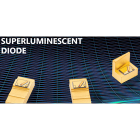

Designed for a wavelength range of 760 to 2900 nm with an accuracy of ±10 nm.

  • Other semiconductors

Added to bookmarks

Bookmarks list

Bookmark has been removed

Bookmarks list

You can't add any more bookmarks

By registering as a member, you can increase the number of bookmarks you can save and organize them with labels.

Free membership registration

QCL optimal for high-precision gas detection using TDLAS.

  • Other semiconductors

Added to bookmarks

Bookmarks list

Bookmark has been removed

Bookmarks list

You can't add any more bookmarks

By registering as a member, you can increase the number of bookmarks you can save and organize them with labels.

Free membership registration

Filter

classification
Delivery Time
Location