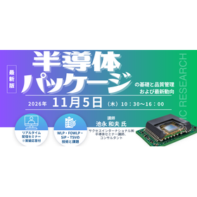
Systematically acquire semiconductor packaging technology from the basics. Learn about quality control and the latest packaging trends in one day.
■Title: "Fundamentals of Semiconductor Packaging, Quality Control, and Latest Trends" ――This course systematically explains the functions and structures required for semiconductor packaging, manufacturing processes, and quality control, as well as the latest technological trends such as SiP, WLP, FOWLP, TSV, chipletization, and three-dimensional packaging. Participants will gain an understanding of the overall landscape of packaging technology and practical challenges, acquiring the knowledge necessary for semiconductor development and manufacturing. - Functions required for semiconductor packaging and technological transitions - Characteristics, challenges, and countermeasures of each subsequent process - Basic knowledge of package quality control - Advanced packaging technologies such as SiP, WLP, FOWLP, TSV - Latest trends in chipletization and three-dimensional packaging - Understanding the interrelation of materials, equipment, and packaging technologies - Young engineers related to packaging technology - Engineers from semiconductor equipment manufacturers and material suppliers - Sales and marketing personnel - Those who wish to systematically acquire knowledge related to semiconductors
Inquire About This Product
basic information
■Event Details Date and Time: November 5, 2026 (Thursday) 10:30 AM - 4:00 PM Participation Fee: 55,000 yen (tax included) *Includes materials *Newsletter subscribers: 49,500 yen (tax included) Instructor: Kazuo Ikenaga (Instructor and Consultant for Semiconductor Seminars at Success International Co., Ltd.) Method of Attendance: This seminar will be a live-streaming seminar using "Zoom." We will provide a comprehensive explanation of packaging technologies, covering functions, structures, manufacturing processes, quality control, and cutting-edge packaging technologies such as WLP, FOWLP, SiP, TSV, and chipletization.
Price information
Participation Fee: 55,000 yen (tax included) *Includes materials *For our newsletter subscribers (registration is free) 49,500 yen (tax included) ★If two or more people apply at the same time and all applicants register as newsletter subscribers, the participation fee per person will be half of the newsletter subscriber price.
Delivery Time
Applications/Examples of results
For details about the program and how to apply, please check the related link URL.
Company information

We provide the latest industrial insights to our clients. By conducting market trend analysis, publishing technology‑related books and research reports, and organizing and managing seminars, we support research and development across a wide range of industries, with a primary focus on manufacturing. Our coverage spans diverse fields such as energy, batteries, chemicals, and biotechnology.
![[Demo Unit Rental] ESD-Compatible Barcode Scanner 'MS851 ESD'](https://image.mono.ipros.com/public/product/image/24c/2000511511/IPROS50291014719946690229.jpeg?w=280&h=280)

![[Semiconductor/Class 100 Compatible] 100% Water-Free Air Nozzle](https://image.mono.ipros.com/public/product/image/2116982/IPROS15202438644694791694.png?w=280&h=280)