
List of Photomask products
- classification:Photomask
1~15 item / All 78 items


It won't break even after 1 million repetitions! A mat switch with reliable operation, high durability, and low price. Suitable for options in machine tools as well. Please consult us about delivery t...
- Sensors


We can accommodate high resistance over 10,000 ohms, with diameters ranging from approximately 30 mm to 8 inches, and we also offer thinning and chip processing arrangements!
- Other semiconductors
- Processing Contract
- Wafer
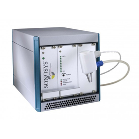

Thorough removal of fine contaminants from wafers. High-quality cleaning achieved by Sonosys.
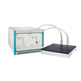
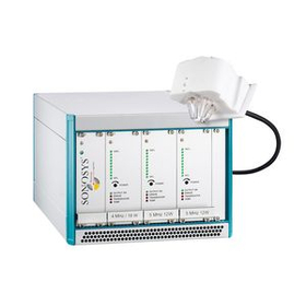
- Ultrasonic Cleaner
- Ultrasonic Oscillator
- Photomask
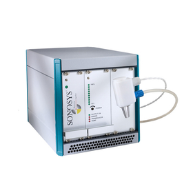
Announcement of the release of the latest leaflet for the SONOSYS Corporation's megasonic cleaning device.
We have updated the product leaflet for the SONOSYS megasonic cleaning device from Germany to the latest version. SONOSYS's megasonic cleaning technology is a non-contact precision cleaning technique that efficiently removes fine particles by transmitting high-frequency ultrasonic energy through liquids such as pure water (DI Water) to the surface of the target object. It is particularly suitable for the precision cleaning of products with fine structures, such as semiconductor wafers, photomasks, MEMS, various substrates, and optical components, and is utilized in various fields that require high cleanliness, starting with semiconductor manufacturing processes. SONOSYS offers a range of frequencies depending on the application and the particles to be removed, as well as a megasonic nozzle system that accommodates various cleaning conditions, including Single Nozzle, Dual Nozzle, and Triple Nozzle. Customers who have challenges such as "wanting to remove fine particles from wafers," "wanting to clean photomasks and MEMS while minimizing damage," or "wanting to review existing cleaning processes" are encouraged to take a look at the latest leaflet.
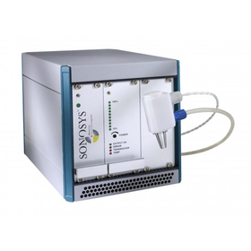
For precise cleaning of prisms. Sonosys ultrasonic cleaning device.
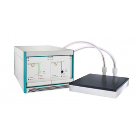
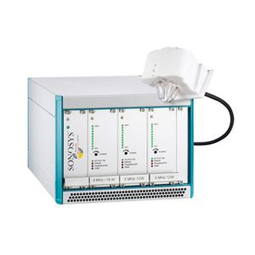
- Ultrasonic Cleaner
- Ultrasonic Oscillator
- Photomask
Announcement of the release of the latest leaflet for the SONOSYS Corporation's megasonic cleaning device.
We have updated the product leaflet for the SONOSYS megasonic cleaning device from Germany to the latest version. SONOSYS's megasonic cleaning technology is a non-contact precision cleaning technique that efficiently removes fine particles by transmitting high-frequency ultrasonic energy through liquids such as pure water (DI Water) to the surface of the target object. It is particularly suitable for the precision cleaning of products with fine structures, such as semiconductor wafers, photomasks, MEMS, various substrates, and optical components, and is utilized in various fields that require high cleanliness, starting with semiconductor manufacturing processes. SONOSYS offers a range of frequencies depending on the application and the particles to be removed, as well as a megasonic nozzle system that accommodates various cleaning conditions, including Single Nozzle, Dual Nozzle, and Triple Nozzle. Customers who have challenges such as "wanting to remove fine particles from wafers," "wanting to clean photomasks and MEMS while minimizing damage," or "wanting to review existing cleaning processes" are encouraged to take a look at the latest leaflet.
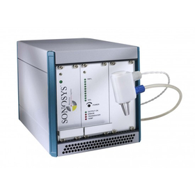
Leave the latest ultrasonic cleaning to Sonosys.


- Photomask
- CMP Equipment
- CVD Equipment
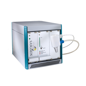
The NHK program "The Wall of Truth" will feature a video of semiconductor wafer cleaning provided by our company.
We are pleased to announce that a video provided by Tick Corporation showcasing semiconductor wafer cleaning will be featured in the NHK program "The Wall of Truth." The theme for this episode is "The Truth of Water (tentative)." The program is scheduled to briefly introduce the process of cleaning wafers with pure water during semiconductor manufacturing. Our company offers cleaning and spraying technologies, including megasonic cleaning, for the semiconductor and electronic components sectors. We are truly honored that our footage will be utilized in the production of this NHK program. Broadcast schedule: September 12, 2026 (Saturday) from 8:30 PM to 8:59 PM (tentative). For more details about the program, please visit the official NHK "The Wall of Truth" page. https://www.nhk.jp/g/ts/N8JX1V6V69/ *Please note that the broadcast date and content may be subject to change.

Next-generation megasonic technology can instantly clear wafers up to 300mm.
- Photomask
- Other semiconductor manufacturing equipment
- Ultrasonic Cleaner
The NHK program "The Wall of Truth" will feature a video of semiconductor wafer cleaning provided by our company.
We are pleased to announce that a video provided by Tick Corporation showcasing semiconductor wafer cleaning will be featured in the NHK program "The Wall of Truth." The theme for this episode is "The Truth of Water (tentative)." The program is scheduled to briefly introduce the process of cleaning wafers with pure water during semiconductor manufacturing. Our company offers cleaning and spraying technologies, including megasonic cleaning, for the semiconductor and electronic components sectors. We are truly honored that our footage will be utilized in the production of this NHK program. Broadcast schedule: September 12, 2026 (Saturday) from 8:30 PM to 8:59 PM (tentative). For more details about the program, please visit the official NHK "The Wall of Truth" page. https://www.nhk.jp/g/ts/N8JX1V6V69/ *Please note that the broadcast date and content may be subject to change.
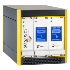
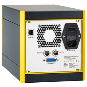
The Digital Generator is a digital control generator compatible with megasonic cleaning systems for semiconductors, electronic components, and precision instruments.
- Photomask
- Other semiconductor manufacturing equipment
- Wafer
The NHK program "The Wall of Truth" will feature a video of semiconductor wafer cleaning provided by our company.
We are pleased to announce that a video provided by Tick Corporation showcasing semiconductor wafer cleaning will be featured in the NHK program "The Wall of Truth." The theme for this episode is "The Truth of Water (tentative)." The program is scheduled to briefly introduce the process of cleaning wafers with pure water during semiconductor manufacturing. Our company offers cleaning and spraying technologies, including megasonic cleaning, for the semiconductor and electronic components sectors. We are truly honored that our footage will be utilized in the production of this NHK program. Broadcast schedule: September 12, 2026 (Saturday) from 8:30 PM to 8:59 PM (tentative). For more details about the program, please visit the official NHK "The Wall of Truth" page. https://www.nhk.jp/g/ts/N8JX1V6V69/ *Please note that the broadcast date and content may be subject to change.
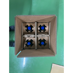

Liquid hazardous materials can also be safely transported with all-fiber solutions.
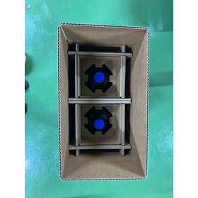
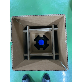
- Wafer
- Resist Device
- Photomask


In grinding, precision management of the pad is important, but are you using a modified carrier that takes into account the type of PAD? Customizing it will also make precision management easier.

- Wafer processing/polishing equipment
- mirror
- Photomask
![[Processing Example] A5052 / Millin...](https://image.mono.ipros.com/public/product/image/20e/2000458177/IPROS16792252807148234778.jpg?w=280&h=280)

Shortest half-day estimate / 【Processing Example】 A5052 / Milling processing / Introduction of black anodizing! Various device parts and machined products can be ordered from just one piece!
- Photomask

[New Catalog Registration] A different approach! A new normal for procurement of processed parts.
<For Designers Who Also Handle Procurement> We propose a new normal procurement method that differs from traditional procurement of processed parts. This is aimed at designers and company presidents who are also involved in the procurement of processed parts, as well as those responsible for procurement and purchasing who may have concerns. 【Contents of the Catalog】 1. "Customer Challenges in Procurement of Processed Parts" 2. "Three Benefits of Assisted Procurement" 2-1. Arrangement of a wide variety of small lots 2-2. Product categories and materials 3. "Overview of Assisted Procurement" 3-1. When the procurement sources are complex 3-2. When the process is long and management is difficult 3-3. Processing sources and added value 3-4. Inspection and quality assurance 4. "Examples of Product Processing" 5. "Company Overview" Please take a look. Feel free to contact us for any inquiries.


It is possible to select an optimal acceleration based on the viscosity of the resist coating agent! We also pay attention to maintainability.
- Photomask

Of course, the airflow control inside the chamber, along with the excellent maintainability of the resist spin coat unit.
- Photomask

Consistent processing of photolithography is possible.
- Photomask

<Semiconductor-related Masks - Basic Information Release> A must-see for those who are handling various masks for the first time due to departmental transfers or job changes! A detailed explanation of...
- Photomask


Samples will be displayed at the exhibition. Improved separation from printed circuit boards! Chemical resistance including organic solvents and alkali.
- Photomask