We have compiled a list of manufacturers, distributors, product information, reference prices, and rankings for microscope.
ipros is IPROS GMS IPROS One of the largest technical database sites in Japan that collects information on.

microscope Product List and Ranking from 173 Manufacturers, Suppliers and Companies | IPROS GMS

Last Updated: Aggregation Period:Jun 17, 2026~Jul 14, 2026
This ranking is based on the number of page views on our site.

microscope Manufacturer, Suppliers and Company Rankings

Last Updated: Aggregation Period:Jun 17, 2026~Jul 14, 2026
This ranking is based on the number of page views on our site.

  1. null/null
  2. フローベル Kanagawa//Optical Instruments
  3. 一般財団法人材料科学技術振興財団 MST Tokyo//Testing, Analysis and Measurement
  4. 4 サーモフィッシャーサイエンティフィック株式会社/Thermo Fisher Scientific K.K. Tokyo//Testing, Analysis and Measurement
  5. 5 レイマー Osaka//Optical Instruments

microscope Product ranking

Last Updated: Aggregation Period:Jun 17, 2026~Jul 14, 2026
This ranking is based on the number of page views on our site.

  1. Exhibiting cutting-edge optical equipment such as dual-sided measurement microscopes for semiconductors and FA, as well as high-speed autofocus. フローベル
  2. White interference microscope equipped with laser 'VK-X4000 series'
  3. All-in-one fluorescence microscope 'BZ-X1000 Series'
  4. 4 White interference microscope equipped with laser microscope 'VK-X3000'
  5. 5 All-in-one fluorescence microscope 'BZ-X800'

microscope Product List

151~180 item / All 668 items

Displayed results

[Analysis Case] STEM, EBSD Image Simulation for Polycrystalline Structure Analysis

Evaluation of crystal forms using simulations.

High-resolution HAADF-STEM images reflect the atomic arrangement of crystals, and by simulating STEM images corresponding to various crystal orientations, they help in accurately understanding the relative orientations between crystal grains and the observed images in polycrystalline materials. This document presents a case where STEM images were simulated from the crystal orientation information obtained by the EBSD method for the crystal grains in a polycrystalline neodymium magnet, and compares them with actual high-resolution HAADF-STEM images.

  • c0557-2.jpg
  • c0557-3.jpg
  • c0557-4.jpg
  • Contract Analysis
  • Contract measurement
  • microscope

Added to bookmarks

Bookmarks list

Bookmark has been removed

Bookmarks list

You can't add any more bookmarks

By registering as a member, you can increase the number of bookmarks you can save and organize them with labels.

Free membership registration

[Analysis Case] TEM Analysis under Atmosphere Control and Cooling (B0156)

Observation with a high-resolution SEM equipped with FIB without atmospheric exposure (controlled atmosphere)!

Our organization has established a system that suppresses atmospheric exposure through atmosphere control, and further cools the samples for processing, observation, and analysis. We can produce TEM thin samples while maintaining the original structure of the specimen, allowing for observation and analysis. Even with unstable materials, we can perform thinning processing while cooling, and by maintaining a vacuum during the transfer between processing and observation devices, we enable cross-sectional TEM/SEM observation that minimizes atmospheric exposure and thermal alteration. 【Measurement and Processing Methods】 ■ [(S)TEM] Scanning Transmission Electron Microscopy ■ Processing under atmosphere control ■ Cryo-processing *For more details, please download the PDF or feel free to contact us.

Added to bookmarks

Bookmarks list

Bookmark has been removed

Bookmarks list

You can't add any more bookmarks

By registering as a member, you can increase the number of bookmarks you can save and organize them with labels.

Free membership registration

[Analysis Case] Dynamic Viscoelastic Evaluation of PDMS using AFM

Introduction to the evaluation of in-plane distribution of viscoelasticity and frequency dependence!

Our organization offers dynamic viscoelastic evaluation of PDMS using AFM. Dynamic Mechanical Analysis (DMA) is an effective method for investigating viscoelastic behavior, which is an important factor in the research and development of polymer materials. Additionally, by combining it with the AFM mechanism, it becomes possible to measure in-plane distribution and evaluate localized areas. This document presents a case study using AFM-DMA to map the viscoelastic modulus of PDMS (polydimethylsiloxane) and conduct frequency-dependent spectroscopy evaluation. [Measurement Method / Processing Method] ■ [AFM] Atomic Force Microscopy *For more details, please download the PDF or feel free to contact us.

Added to bookmarks

Bookmarks list

Bookmark has been removed

Bookmarks list

You can't add any more bookmarks

By registering as a member, you can increase the number of bookmarks you can save and organize them with labels.

Free membership registration

[Analysis Case] (S)TEM Observation by Negative Staining

Examples of morphological observation of liposomes, CNF, microparticles, proteins, etc.!

Our organization offers (S)TEM observation using negative staining. Organic functional materials, such as fine particles and fibrous substances, are primarily composed of light elements like C (carbon), H (hydrogen), O (oxygen), and N (nitrogen), which do not provide sufficient contrast for morphological observation in (S)TEM. Therefore, by applying staining to these materials, we can enhance the contrast and enable observation. In this instance, we will introduce a case where negative staining was performed using phosphotungstic acid (H3[P(W3O10)4]·nH2O, abbreviated as PTA). 【Measurement Method / Processing Method】 ■ [(S)TEM] Scanning Transmission Electron Microscopy ■ Others *For more details, please download the PDF or feel free to contact us.

Added to bookmarks

Bookmarks list

Bookmark has been removed

Bookmarks list

You can't add any more bookmarks

By registering as a member, you can increase the number of bookmarks you can save and organize them with labels.

Free membership registration

OBF STEM method (Optimal Bright Field Scanning Transmission Electron Microscopy)

OBF STEM: Optimum Bright-Field STEM Method

The OBF STEM method is a technique that reconstructs a single STEM image by applying a weighted frequency filter to multiple STEM images obtained from each segment of a segmented STEM detector, appropriately emphasizing different spatial frequency components for each segment. It is characterized by its ability to efficiently utilize the detection signal, allowing for the visualization of structures with low noise and high contrast even under conditions of low electron beam exposure.

  • img_B0310_7.jpg
  • Contract Analysis
  • Secondary Cells/Batteries
  • Memory
  • microscope

Added to bookmarks

Bookmarks list

Bookmark has been removed

Bookmarks list

You can't add any more bookmarks

By registering as a member, you can increase the number of bookmarks you can save and organize them with labels.

Free membership registration

Hamamatsu Photonics PHEMOS-X

Equipped with a multi-wavelength laser, it can handle everything from visible light to near-infrared light with a single device.

PHEMOS-X is a high-resolution emission microscope that captures light emission and heat generation caused by semiconductor device failures to identify the failure location. 1. Capable of mounting up to two ultra-high sensitivity cameras. 2. Can accommodate up to seven light sources for OBIRCH, DALS, EOP, and laser markers. 3. Equipped with an optical stage compatible with various samples.

  • Optical microscope
  • microscope

Added to bookmarks

Bookmarks list

Bookmark has been removed

Bookmarks list

You can't add any more bookmarks

By registering as a member, you can increase the number of bookmarks you can save and organize them with labels.

Free membership registration

Confocal Microscopy Laser Raman "SENTERRA II"

[Technical Data Presentation] Achieving high sensitivity performance and high frequency accuracy! A compact and robust distributed micro-Raman system.

The "SENTERRA II" is a high-performance system unique to Bruker, capable of handling everything from routine analyses such as quality control to cutting-edge research fields. In typical Raman microscopes, the spectrometer is mostly a separate system from the microscope, requiring a significant amount of time to maintain performance. This product is a compact and robust integrated system that combines the excitation laser, spectrometer, and microscope, achieving high performance and stability through its efficient optical design. Additionally, it supports operators smoothly and accurately to obtain results quickly. It guides users step by step through the procedures of data measurement, from visual observation of samples to confirming spectral quality and setting measurement areas. [Features] - Highly automated various functions and efficient operability - Compact & robust design - Efficiency and flexibility *For more details, please refer to the PDF document or feel free to contact us.

  • Analytical Equipment and Devices
  • microscope

Added to bookmarks

Bookmarks list

Bookmark has been removed

Bookmarks list

You can't add any more bookmarks

By registering as a member, you can increase the number of bookmarks you can save and organize them with labels.

Free membership registration

Technical Data: Analysis of Large Samples Using FTIR Microscopy

Introduction of application examples for the analysis of long needle tips made of metal and the analysis of large automotive parts.

The fully automatic FTIR microscope "LUMOS II" allows for direct analysis of large samples without the need for tedious sample pretreatment. The size and range of the sample stage, as well as the working distance, are very important factors in microscopic analysis. By using accessories such as vice holders according to the sample shape, it is also possible to easily analyze challenging samples, such as needle tips. 【Contents】 ■ Introduction ■ Equipment ■ Application Example: Analysis of the tip of a long metal needle ■ Application Example: Analysis of large automotive parts ■ Conclusion *For more details, please refer to the PDF document or feel free to contact us.

Added to bookmarks

Bookmarks list

Bookmark has been removed

Bookmarks list

You can't add any more bookmarks

By registering as a member, you can increase the number of bookmarks you can save and organize them with labels.

Free membership registration

FT-IR and QCL Microscope "HYPERION II Series"

A research and development FT-IR microscope with flexible expandability. It is possible to incorporate imaging functions using QCL infrared lasers into a single device.

HYPERION II is a technological innovation in infrared microscopy. It has achieved diffraction-limited infrared imaging and set a standard in micro ATR. Furthermore, it is the world's first system that integrates both FT-IR microscopy and infrared laser imaging microscopy (ILIM) functionalities in a single device for all measurement modes: transmission, reflection, and ATR. *For more details, please refer to the PDF document or feel free to contact us.*

  • Spectroscopic Analysis Equipment
  • microscope

Added to bookmarks

Bookmarks list

Bookmark has been removed

Bookmarks list

You can't add any more bookmarks

By registering as a member, you can increase the number of bookmarks you can save and organize them with labels.

Free membership registration

[Technical Data] High-Throughput Screening of Surface Contamination

A dramatic improvement in operational efficiency is expected, as well as new applications!

The infrared microscope "HYPERION II" supports infrared laser imaging using QCL in addition to conventional micro FT-IR measurements. This document includes topics such as "QA/QC of precision machinery using FT-IR," "rapid detection of Regions of Interest (ROI)," and "detection of ROI using infrared laser imaging." The combination of QCL and FT-IR enables the swift detection of ROIs and more accurate qualitative analysis based on that information. [Contents] ■ QA/QC of precision machinery using FT-IR ■ Rapid detection of Regions of Interest (ROI) ■ Benefits of the combination of FT-IR and QCL ■ Detection of ROI using infrared laser imaging ■ Improved reliability of analysis using FT-IR ■ FT-IR and laser imaging: a powerful combination *For more details, please refer to the PDF document or feel free to contact us.

Added to bookmarks

Bookmarks list

Bookmark has been removed

Bookmarks list

You can't add any more bookmarks

By registering as a member, you can increase the number of bookmarks you can save and organize them with labels.

Free membership registration

Forensic Analysis of Automotive Paint Samples Using QCL and FT-IR

It is possible to analyze even tiny fragments of paint! In fact, it contributes to identifying accident vehicles.

The infrared microscope is one of the analytical tools capable of identifying the composition of microscopic objects and has become indispensable in forensic evidence analysis. The analysis method introduced in this document, using Bruker's "HYPERION II-ILIM System," combines IR laser imaging and micro FT-IR measurement, significantly reducing analysis time while further improving the quality of analysis. Please feel free to download and take a look. 【Contents】 ■ Differences in light sources used for IR laser imaging and FT-IR ■ Analysis method combining IR laser imaging and FT-IR ■ Application example: Automotive paint chips ■ Game changer: Achieving IR laser imaging and FT-IR measurement in a single device ■ Measurement results: Improved efficiency and reliability *For more details, please refer to the PDF document or feel free to contact us.

  • Spectroscopic Analysis Equipment
  • microscope

Added to bookmarks

Bookmarks list

Bookmark has been removed

Bookmarks list

You can't add any more bookmarks

By registering as a member, you can increase the number of bookmarks you can save and organize them with labels.

Free membership registration

Technical Data: Analysis of Particles Contained in Injectable Preparations

Utilization of micro FT-IR imaging measurement method! It is possible to identify the chemical composition of samples with high precision.

FT-IR microscopy not only provides high resolution but also offers comprehensive chemical information that is useful for identifying discovered particles. This reveals the chemical composition of spatially defined areas of the sample, and USP <788> and USP <787> recognize FT-IR microspectroscopy as a suitable tool for the characterization of invisible particles in therapeutic protein injectables. This document presents two measurement examples using FT-IR microscopy and its imaging capabilities for the identification of particles in solution formulations. We encourage you to read it. [Contents (partial)] ■ Why focus on particles? ■ What are the regulations regarding particles? ■ How are particles detected? ■ Application Example 1 ■ Application Example 2 *For more details, please refer to the PDF document or feel free to contact us.

Added to bookmarks

Bookmarks list

Bookmark has been removed

Bookmarks list

You can't add any more bookmarks

By registering as a member, you can increase the number of bookmarks you can save and organize them with labels.

Free membership registration

Case Study Collection 1 on Cross-Section Observation and Structural Analysis using TEM/SEM/EBSD

We will introduce many examples of cross-sectional observation and structural analysis using TEM, FE-SEM, EBSD, etc., for metal microstructure observation and phase analysis!

This case study collection introduces examples related to "cross-sectional observation and structural analysis." It includes numerous analytical cases covering the objectives, methods, and results of "metallic structure observation of wire (spring material)," "phase analysis of duplex stainless steel," and "evaluation of semiconductor insulating films using STEM-EDS." Additionally, it presents observations, phase analyses, insulating film analyses, and measurements, among other topics. We encourage you to read it. [Contents] ■ Metallic structure observation of wire (spring material) ■ Phase analysis of duplex stainless steel ■ Evaluation of semiconductor insulating films using STEM-EDS ■ EBSD measurement of samarium cobalt magnets ■ Analysis of connector terminal contact defects using STEM ■ Cross-sectional observation of biological samples (Morpho butterfly scales) *For more details, please refer to the PDF document or feel free to contact us.

  • Other analyses
  • Contract Analysis
  • Contract Analysis
  • microscope

Added to bookmarks

Bookmarks list

Bookmark has been removed

Bookmarks list

You can't add any more bookmarks

By registering as a member, you can increase the number of bookmarks you can save and organize them with labels.

Free membership registration

Conductivity evaluation of plated contact component surfaces 【DL available/AFM】

AFM can capture and measure extremely small surface topographies (roughness).

The AFM scanning probe microscope is a device that "detects various physical interactions between the probe and the sample surface, allowing for the observation of surface shapes in minute areas and the measurement of electrical and mechanical properties." These physical interactions include atomic forces, frictional forces, and electrostatic forces. Additionally, measurements can be taken in various environments, including atmospheric and vacuum conditions, enabling the observation of sample surfaces regardless of conductivity or insulation. Using this analytical device, we conducted an investigation into the "surface treatment of plated connector contact parts." Please take a moment to read the PDF materials. Furthermore, in addition to this analytical device, our company also conducts various surface analyses such as XPS, AES, and GD-OES. We would be happy to assist you, so please feel free to reach out. Seiko Future Creation Official Website https://www.seiko-sfc.co.jp/ *We have many other achievements as well. If you request through the inquiry button, we will send them to you.

  • Plating Equipment
  • Contract Analysis
  • Electrical Instruments/Electrometers
  • microscope

Added to bookmarks

Bookmarks list

Bookmark has been removed

Bookmarks list

You can't add any more bookmarks

By registering as a member, you can increase the number of bookmarks you can save and organize them with labels.

Free membership registration

EPIScope

We have commercialized the "EPIScope," a tabletop microscope type of EPIS sensor, so that customers can easily use it.

1. It can identify the "defective location" of Open/Short, which is difficult to determine with electrical testing. 2. It can detect "dents" that are difficult to identify with optical images. 3. It can detect defects not only in surface patterns but also in internal layer patterns. 4. It allows for dynamic observation as well as static images. 5. Since it detects electrical differences, it is less affected by dirt (insulators).

  • Circuit Board Inspection Equipment
  • microscope

Added to bookmarks

Bookmarks list

Bookmark has been removed

Bookmarks list

You can't add any more bookmarks

By registering as a member, you can increase the number of bookmarks you can save and organize them with labels.

Free membership registration

CIQTEK Scanning NV Microscope

CIQTEK CIQTEK Scanning NV Microscope

CIQTEK QDAFM - Diamond III is a magnetic imaging device that combines the diamond NV center with AFM imaging technology. Through quantum control and spin detection using a diamond probe, the magnetic properties of samples can be obtained quantitatively and non-invasively. With nanoscale spatial resolution and ultra-high detection sensitivity, QDAFM is an innovative technology for researching and developing magnetic textures, high-density magnetic storage, and spintronics. The magnetic imaging technology enabled by quantum probes equipped with diamond NV centers provides a new means of measuring magnetic fields with high spatial resolution and excellent sensitivity. This scanning NV center magnetometer not only scans magnetic materials but also extends its applications to important areas such as the study of mechanisms in biomolecules, life sciences, healthcare diagnostics, and disease treatment.

  • Electron microscope
  • Other microscopes
  • Other measurement, recording and measuring instruments
  • microscope

Added to bookmarks

Bookmarks list

Bookmark has been removed

Bookmarks list

You can't add any more bookmarks

By registering as a member, you can increase the number of bookmarks you can save and organize them with labels.

Free membership registration

Penscope 8x Telescope & 30x Microscope PS-30N

8x telescope and 30x microscope. When using the microscope, the image will be inverted.

8x telescope & 30x microscope. When using the microscope, the image will be inverted.

  • Microscope
  • microscope

Added to bookmarks

Bookmarks list

Bookmark has been removed

Bookmarks list

You can't add any more bookmarks

By registering as a member, you can increase the number of bookmarks you can save and organize them with labels.

Free membership registration

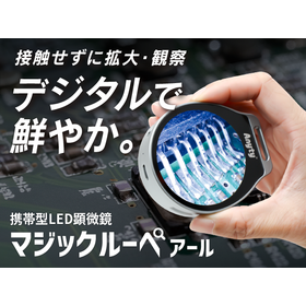
800x Magnification Portable Digital Microscope (Infrared Model) [Demo Unit Available for Loan]

Portable digital microscope with a maximum magnification of 800x, available in infrared/ultraviolet models.

A digital microscope with a monitor-integrated type that can be carried and used anywhere. It can magnify up to 800 times and allows for the capture and storage of still images and videos. <Product Features> 1. Choose between infrared and ultraviolet models according to your needs. 2. A full-fledged microscope that is portable. 3. Maximum magnification of 800 times. 4. Comes with a wired controller that is great for preventing hand shake. 5. Simple scale display available. 6. Data can be saved to an SD card. *Demo units are available for those who want to try the product. *Offered at a price suitable for budget consumption.

  • Microscope
  • microscope

Added to bookmarks

Bookmarks list

Bookmark has been removed

Bookmarks list

You can't add any more bookmarks

By registering as a member, you can increase the number of bookmarks you can save and organize them with labels.

Free membership registration

Wireless digital microscope compatible with up to 600x magnification via WIFI [Demo units available for loan].

[Demo unit available for loan] The magnified images displayed by the microscope body can be projected to smartphones and tablets via WIFI. It can magnify up to 600 times.

A digital microscope that can be used wirelessly with a WIFI connection. It transmits images captured by the microscope body wirelessly to your smartphone or tablet. ○ Wireless digital microscope There is no need to connect with cables like wired models, so cables won't get in the way. Additionally, with wired models, certain locations may be hard to reach due to cable length, or there may be environments without power where use is not possible. However, with a wireless digital microscope, you can easily use it in such situations. ○ WIFI connection for observation on tablets and smartphones This product adopts "WIFI connection" among wireless options. Therefore, it can wirelessly transmit images to tablets and smartphones equipped with WIFI functionality. It can be used with both Android and iOS devices, as well as with computers that have wireless capabilities. ○ Capability to capture videos/still images, save data, and perform measurements It is possible to capture videos (iOS only) and still images, as well as save data. Furthermore, you can correct and measure the captured images, and the measurement results can be saved as data. This can be utilized for creating documents and other purposes. *For those who would like to try the product, we have a [demo unit available for loan].

  • Microscope
  • microscope

Added to bookmarks

Bookmarks list

Bookmark has been removed

Bookmarks list

You can't add any more bookmarks

By registering as a member, you can increase the number of bookmarks you can save and organize them with labels.

Free membership registration

No need to peek! Project the microscope images onto your PC's large screen.

[Free demo units available] Wirelessly enlarge and save the images displayed by the microscope on your computer.

【Free Demo Units Available】The 'Wireless Digital Microscope PC Model (3R-WM401PC)' uses a 2.4GHz frequency band for wireless transmission, allowing the images viewed through the microscope to be displayed on a computer. (Magnification: 1x to 200x) Being a wireless type, it can be used without being limited by the environment, making it suitable for fieldwork and various on-site applications. It enables detailed observation of work-related issues such as scratches, burrs, and foreign matter, making it valuable for quality control in factories. There is also a dedicated monitor model (3R-WM401TV), allowing for model selection based on specific applications. It has obtained technical standard conformity certification and is offered at a price suitable for budget consumption. 【Features】 ■ Real-time wireless transmission of images to a computer ■ Supports high magnification up to 200x, comparable to a professional microscope ■ Dedicated software allows for measurement and correction of captured images ■ Supports both still images and video recording

  • Microscope
  • microscope

Added to bookmarks

Bookmarks list

Bookmark has been removed

Bookmarks list

You can't add any more bookmarks

By registering as a member, you can increase the number of bookmarks you can save and organize them with labels.

Free membership registration

600x Wireless Digital Microscope PC Model Measurement Available [Demo Unit for Loan]

[Demo unit available for loan] Display and save 600x magnified images from the microscope body wirelessly on a computer.

[Demo unit available for loan] [3R-WM601PC] is a wireless digital microscope that uses a 2.4GHz frequency band to transmit images captured by the microscope body to a computer. (Magnification: 450-600 times) Being a wireless type, it can be used in various environments without restrictions, such as on-site or fieldwork. It allows for detailed observation of work-related issues like scratches, burrs, and foreign matter, making it useful for quality control in factories. There is also a dedicated monitor model (3R-WM601TV), allowing for model selection based on specific applications. It has obtained technical standards compliance certification and is offered at a price suitable for budget consumption. [Features] ■ Real-time transmission of images to a computer via wireless connection ■ Supports high magnification up to 450-600 times, comparable to a professional microscope ■ Dedicated software allows for measurement and correction of captured images ■ Supports both still images and video recording

  • Microscope
  • microscope

Added to bookmarks

Bookmarks list

Bookmark has been removed

Bookmarks list

You can't add any more bookmarks

By registering as a member, you can increase the number of bookmarks you can save and organize them with labels.

Free membership registration

200x Wireless Digital Microscope Mobile TV Model [Demo Unit Available for Loan]

[Demo unit available for loan] Displays and saves enlarged images captured by the microscope on a dedicated mobile monitor.

[Demo Unit Available for Loan] The [3R-WM401TV] is a wireless digital microscope that uses a 2.4GHz frequency band to transmit images captured by the microscope body to a dedicated mobile monitor. (Magnification: 1x to 200x) Being a wireless type, it has no cables, allowing it to be used anywhere without being limited by the environment, such as in fieldwork. It is effective for observing details such as scratches, burrs, and foreign matter, making it useful for quality control in factories. There is also a computer model (3R-WM401PC) available, allowing for model selection based on specific applications. It has obtained technical standards compliance certification and is offered at a price suitable for budget consumption. [Features] ■ Real-time image transmission to the monitor via wireless connection ■ Supports high magnification up to 200x, comparable to a professional microscope ■ Multiple monitors can be connected simultaneously ■ Supports both still images and video recording ■ Can be connected to a TV screen for observation on a large display

  • Microscope
  • microscope

Added to bookmarks

Bookmarks list

Bookmark has been removed

Bookmarks list

You can't add any more bookmarks

By registering as a member, you can increase the number of bookmarks you can save and organize them with labels.

Free membership registration

HDMI output digital microscope that magnifies clearly with high magnification and high resolution.

Since it is non-contact, observation and photography can be done without causing scratches or dirt on the subject. Delicate objects can also be observed safely.

The 【3R-MSTVUSB273】 is a digital microscope equipped with HDMI mode and PC mode, supporting a maximum magnification of up to 273 times (in HDMI mode/C mode). It allows for the magnification, inspection, and saving of non-contact and delicate objects that cannot be touched or damaged. The sensor has a resolution of 5 million pixels and supports the previously limited output resolution of "1080p" in HDMI mode, displaying digital images clearly. In PC mode, it supports functions for shooting, measuring, and editing, allowing edited images to be saved directly. In HDMI mode, magnification can also be calculated with this device, and a simple visual confirmation of the actual size scale is possible. 【Features】 ■ Non-contact design allows for the observation of delicate objects ■ Two observation modes: HDMI mode and PC mode ■ Magnification and focus can be adjusted by changing the height of the stand ■ Image capturing, editing, and measuring capabilities (PC mode only) ■ Auto-focus function (PC mode only)

  • Microscope
  • microscope

Added to bookmarks

Bookmarks list

Bookmark has been removed

Bookmarks list

You can't add any more bookmarks

By registering as a member, you can increase the number of bookmarks you can save and organize them with labels.

Free membership registration

Camera-equipped infrared microscope 'InGaAs'

Built-in LED ring dark field infrared illumination! Enables easy high-resolution infrared microscopy imaging.

The "InGaAs" is an infrared microscope equipped with a camera that features built-in LED ring dark field infrared illumination, allowing for easy high-resolution infrared imaging. When using a near-infrared camera as a microscope, it consists of an accessory set including a tube, objective lens, infrared LED illumination, and power supply. 【Features】 ■ Built-in LED ring dark field infrared illumination ■ Easy high-resolution infrared imaging ■ Magnification: x20 (also compatible with x10 and x50) ■ Focal length: 95mm ■ Working distance: 20mm *For more details, please refer to the PDF document or feel free to contact us.

  • Other microscopes
  • microscope

Added to bookmarks

Bookmarks list

Bookmark has been removed

Bookmarks list

You can't add any more bookmarks

By registering as a member, you can increase the number of bookmarks you can save and organize them with labels.

Free membership registration

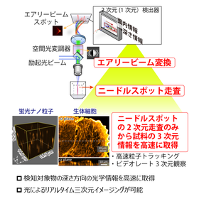
SPR Microscope

A fusion system of intermolecular interaction analysis and bright field imaging!

The "SPR Microscope" is an innovative system that simultaneously analyzes molecular interactions using surface plasmon resonance (SPR) and performs imaging in bright field. It is designed as a system to measure the binding activity and cellular dynamics of membrane proteins on cells in a label-free manner under in vitro conditions. As a result, it can simultaneously acquire the distribution of binding activity (SPR two-dimensional mapping images) and cellular structure (bright field images), allowing for the investigation of changes at the cellular level. 【Features】 ■ Fusion of molecular interaction analysis device and optical microscope ■ Mapping of label-free binding activity at the cellular level under in vitro conditions ■ Measurement of binding responses of bacteria, viruses, and nanoparticles at the nanometer level * This PDF document is the English version. * For more details, please refer to the PDF document or feel free to contact us.

  • Other microscopes
  • microscope

Added to bookmarks

Bookmarks list

Bookmark has been removed

Bookmarks list

You can't add any more bookmarks

By registering as a member, you can increase the number of bookmarks you can save and organize them with labels.

Free membership registration

Technical Information Magazine 202305-02 In-situ Heating TEM

Using in-situ heating TEM, we introduce a case study that visualizes structural changes in materials at the nanometer level during thermal processing of semiconductor devices, contributing to process development.

The technical information magazine The TRC News provides the latest information on analytical techniques that are useful for research and development, solving production troubles, and quality control. **Abstract** In the development and manufacturing of semiconductor devices, understanding the structural changes of materials during thermal processing is extremely important. By using heating in-situ TEM, it is possible to visualize the thermal behavior of materials during heat treatment at the nanometer level, gaining new insights into structural changes that can aid in process development such as film quality control. This paper introduces case studies using heating in-situ TEM to analyze (1) the crystallization growth mechanism of amorphous silicon films in conjunction with crystal structure analysis, (2) the thermal behavior of metal stacked films in conjunction with elemental analysis, and (3) the observation of the crystallization growth process of thin film ruthenium films in a planar configuration. **Table of Contents** 1. Introduction 2. Overview and Features of Heating In-Situ TEM 3. Case Studies of Heating In-Situ TEM Analysis 4. Conclusion

  • Contract Analysis
  • Contract measurement
  • Technical and Reference Books
  • microscope

Added to bookmarks

Bookmarks list

Bookmark has been removed

Bookmarks list

You can't add any more bookmarks

By registering as a member, you can increase the number of bookmarks you can save and organize them with labels.

Free membership registration