We have compiled a list of manufacturers, distributors, product information, reference prices, and rankings for Electron microscope.
ipros is IPROS GMS IPROS One of the largest technical database sites in Japan that collects information on.

Electron microscope Product List and Ranking from 35 Manufacturers, Suppliers and Companies | IPROS GMS

Last Updated: Aggregation Period:Jul 08, 2026~Aug 04, 2026
This ranking is based on the number of page views on our site.

Electron microscope Manufacturer, Suppliers and Company Rankings

Last Updated: Aggregation Period:Jul 08, 2026~Aug 04, 2026
This ranking is based on the number of page views on our site.

  1. アズサイエンス 松本本社 Nagano//Trading company/Wholesale
  2. 一般財団法人材料科学技術振興財団 MST Tokyo//Testing, Analysis and Measurement
  3. アイテス Shiga//Electronic Components and Semiconductors
  4. 4 ロンビック Mie//Resin/Plastic
  5. 5 大同分析リサーチ Aichi//Service Industry

Electron microscope Product ranking

Last Updated: Aggregation Period:Jul 08, 2026~Aug 04, 2026
This ranking is based on the number of page views on our site.

  1. Research on polymer materials, foreign substance analysis and quality control in pharmaceuticals, electronics, and chemical fields! アズサイエンス 松本本社
  2. Announcement of the introduction of Talos F200E アイテス
  3. JSM-IT800 Field Emission Scanning Electron Microscope アズサイエンス 松本本社
  4. 4 Observation of Cellulose Nanofibers (CNF) - Examples of SEM and TEM Observations ロンビック
  5. 5 [Slice&View] Three-Dimensional SEM Observation Method 一般財団法人材料科学技術振興財団 MST

Electron microscope Product List

151~164 item / All 164 items

Displayed results

Introduction of recommended products from Azusa Science.

It can be utilized in various fields such as medicine, biology, metals, semiconductors, and ceramics.

Here, we introduce three products from Japan Electron Optics Laboratory Co., Ltd., recommended by Azusa Science, which are electron microscopes. ■ JSM-IT200 InTouchScope Scanning Electron Microscope The features of this higher-end model have been simplified for easier use. With a user-friendly sample exchange guide, it allows for easy sample setup, finding the field of view, and starting SEM image observation. It integrates software for analytical tasks. ■ JCM-7000 NeoScope Desktop Scanning Electron Microscope With the concept of "Anyone can operate SEM/EDS," it meets the needs for improved work efficiency, ease of operation, and enhanced analysis and measurement performance. Placing one next to an optical microscope allows for faster and more detailed foreign object analysis and quality control. ■ JSM-IT510 InTouchScope Scanning Electron Microscope In quality assurance and manufacturing environments, it is necessary to repeatedly perform the same observation tasks, leading to demands for process efficiency. The JSM-IT510 features a newly added Simple SEM function that allows for "hands-free" repetitive tasks. It has become easier and more efficient to conduct SEM observation tasks.

  • JSM-IT200 InTouchScope? 走査電子顕微鏡.png
  • JSM-IT510 InTouchScope? 走査電子顕微鏡.png
  • Electron microscope
  • Electron microscope

Added to bookmarks

Bookmarks list

Bookmark has been removed

Bookmarks list

You can't add any more bookmarks

By registering as a member, you can increase the number of bookmarks you can save and organize them with labels.

Free membership registration

For research in organic chemistry and materials science, as well as observations at atomic resolution!

Introduction to recommended electron microscopes, polarizing microscopes, and mass spectrometers by Azusa Science.

Here are three recommended products: ◆ JEOL Ltd. JEM-ARM200F NEOARM Atomic Resolution Analytical Electron Microscope Equipped with a cold field emission gun (Cold-FEG) and a new spherical aberration corrector (ASCOR) capable of correcting higher-order aberrations as standard, it enables atomic resolution observation not only at a high acceleration voltage of 200 kV but also at a low acceleration voltage of 30 kV. This makes it easier to observe materials containing light elements with clear contrast. ◆ Nikon Solutions Co., Ltd. Polarized/Dispersion Microscope ECLIPSE LV100ND POL/DS This microscope can measure the properties of asbestos, such as refractive index, birefringence, retardation, extinction angle, pleochroism, and elongation, aiding in the identification of asbestos. It allows for dispersion staining observation at a magnification of 400 times. ◆ JEOL Ltd. JMS-T100LP AccuTOF LC-Express Atmospheric Pressure Ionization Time-of-Flight Mass Spectrometer This high-throughput mass spectrometer aims for high productivity with features such as multi-ionization, robustness, and easy maintenance. It is capable of analyzing a wide range of samples from low polarity to high polarity.

  • JEM-ARM200F.png
  • JMS-T100LP.png
  • ECLIPSE LV100ND POL-DS.png
  • Analytical Equipment and Devices
  • Electron microscope

Added to bookmarks

Bookmarks list

Bookmark has been removed

Bookmarks list

You can't add any more bookmarks

By registering as a member, you can increase the number of bookmarks you can save and organize them with labels.

Free membership registration

Fundamentals and Applications of MicroED Crystal Structure Analysis Part 2 (Held on 10/15)

Free participation! Report on the determination of absolute stereochemistry using MicroED.

We will hold a webinar titled "Fundamentals and Applications of MicroED Crystal Structure Analysis Part 2 - Determining Absolute Stereochemistry Using MicroED." This time, referred to as "Part 2," we will introduce the determination of "absolute stereochemistry" while fully considering the effects of multiple scattering of electrons. This method is an excellent technique that demonstrates remarkable power in determining absolute stereochemistry in molecules composed solely of light elements. As a case study, this webinar will report on the determination of absolute stereochemistry using MicroED for complex natural products and synthetic pharmaceutical raw materials. [Event Overview] ■ Date and Time: October 15, 2024 (Tuesday) 14:00 - 14:45 ■ Participation: Free ■ Venue: Webinar held via Microsoft Teams *For more details, please refer to the related links or feel free to contact us.

  • Structural analysis contract
  • Seminar
  • Electron microscope

Added to bookmarks

Bookmarks list

Bookmark has been removed

Bookmarks list

You can't add any more bookmarks

By registering as a member, you can increase the number of bookmarks you can save and organize them with labels.

Free membership registration

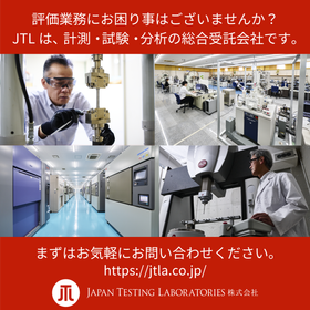
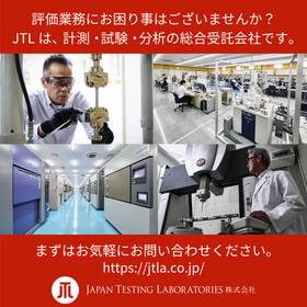
Contracted service for cross-section sample polishing | JTL

We will create cross-section samples for analysis and observation according to your request.

We will carry out the necessary sample preparation processes for observing the cross-sections of solder joints and welds, analyzing the cross-sections of foreign objects, and confirming the interiors of assembly products, including "cutting the target object → resin embedding → polishing." We accept requests for sample preparation alone, as well as comprehensive services that include observation and analysis after preparation. - Polyester resin Used for embedding large products Does not contain chlorine in the resin - Acrylic resin High transparency Resistant to scratches - Epoxy resin Has a low curing shrinkage rate and is less prone to cracking (catalog value 0.5%) Excellent heat, water, chemical, and weather resistance Superior adhesion to non-substrates Contains trace amounts of chlorine in the resin - Polisher Short production time for cross-section samples (fewer steps to mirror polishing) Mainly used for polishing resin materials and steel materials. - Precision polisher Allows for setting polishing pressure and time. Can suppress distortion even when polishing hard materials such as carbide and ceramics.

  • Other services
  • Processing Contract
  • Plastic processing machines (cutting and rolling)
  • Electron microscope

Added to bookmarks

Bookmarks list

Bookmark has been removed

Bookmarks list

You can't add any more bookmarks

By registering as a member, you can increase the number of bookmarks you can save and organize them with labels.

Free membership registration

Analysis of high-performance materials with 'Materials Studio'

Analysis simulation of high-performance materials, as well as material development simulation software compatible with various types of materials.

"Materials Studio" A suite of molecular modeling/simulation tools for next-generation materials development equipped with quantum mechanics (density functional theory), classical mechanics (molecular dynamics calculations), mesoscale (dissipative particle dynamics calculations, etc.), statistics, and analysis/crystallization tools. 【Features】 ■ Simulation software that streamlines materials development Available for use by those engaged in research, development, design, and manufacturing across various industries and fields. ■ Compatible with various types of materials ■ All tasks, including crystal structure creation, calculation condition settings, and calculation result display, can be performed on a single GUI screen. 【Examples】 Tribochemical (lubrication) reactions Analysis of CFRP (carbon-based materials) Research and development of crystal growth, thin film formation, fuel cells, lubricants, etc. Catalysts, polymers and mixtures, metals and alloys, batteries and fuel cells, etc. *For more details, please feel free to contact us.*

  • others
  • Image analysis software
  • Electron microscope

Added to bookmarks

Bookmarks list

Bookmark has been removed

Bookmarks list

You can't add any more bookmarks

By registering as a member, you can increase the number of bookmarks you can save and organize them with labels.

Free membership registration

[Market Report] World Market for Scanning Electron Microscopes

The global market for scanning electron microscopes is expected to drive scientific discoveries and experience significant growth.

The global market for scanning electron microscopes (SEM) is at the forefront of scientific exploration, achieving approximately $3.83 billion in revenue in 2022. Industry experts predict that this market will reach $7.84 billion in sales by 2031. This forecast implies a compound annual growth rate (CAGR) of 8.3% during the forecast period from 2023 to 2031. Scanning electron microscopes serve as a window into the microscopic world, revealing complex details of structures and materials that are not visible to the naked eye. From fundamental research to advanced industrial applications, SEMs are essential tools for scientists, engineers, and researchers to unravel minute mysteries. For application methods, please check the [PDF download] button or apply directly through the related links.

  • others
  • Electron microscope

Added to bookmarks

Bookmarks list

Bookmark has been removed

Bookmarks list

You can't add any more bookmarks

By registering as a member, you can increase the number of bookmarks you can save and organize them with labels.

Free membership registration

Contracted service for ion milling processing | JTL

We will produce cross-sectional samples without any taper using the ion milling method.

We will perform precise sample preparation necessary for high-magnification observation using the ion milling method for cross-sectional processing. In conventional mechanical polishing using polishing paper and abrasives, issues such as deformation due to stress during polishing, collapse of voids, and cracking could occur. Even for samples prone to such phenomena, by performing polishing with a very weak ion beam, we can produce cross-sectional samples suitable for high-magnification observation and analysis of micro-regions, as well as crystal orientation analysis (EBSD).

  • Other services
  • Processing Contract
  • Surface treatment contract service
  • Electron microscope

Added to bookmarks

Bookmarks list

Bookmark has been removed

Bookmarks list

You can't add any more bookmarks

By registering as a member, you can increase the number of bookmarks you can save and organize them with labels.

Free membership registration

[Column] The Difference Between Digital Microscopes and Electron Microscopes

What is the difference between a digital microscope and an electron microscope? It is important to choose the right equipment.

The electron microscope and digital microscope each have different areas of observation in which they excel. If you choose one without knowing their respective features and usability, you may not be able to conduct observations that align with your intentions. This column introduces the characteristics and differences between digital microscopes and electron microscopes. If you are unsure which one to implement, please use this as a reference. For more details, please see the related links. [Content Included] ■ Characteristics of digital microscopes and electron microscopes ■ Differences between digital microscopes and electron microscopes ■ Choose the one suited for each application *You can view the detailed content of the column (such as blogs) from the related links. For more information, please feel free to contact us.

  • Microscope
  • Electron microscope

Added to bookmarks

Bookmarks list

Bookmark has been removed

Bookmarks list

You can't add any more bookmarks

By registering as a member, you can increase the number of bookmarks you can save and organize them with labels.

Free membership registration