September 29 Webinar "Semiconductor Packaging and Encapsulation Technology"
 CMC RESEARCH Ltd.
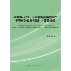
■Title: "Latest Trends in Semiconductor Packaging and Design/Evaluation Techniques for Semiconductor Encapsulation Materials"
--- This seminar systematically explains encapsulation materials that correspond to evolving semiconductor packages such as chiplets and 3D packages, covering everything from raw materials like epoxy resins, hardeners, and additives to design and evaluation. It will also introduce technological trends for next-generation encapsulation materials, including low dielectric, high thermal conductivity, and optoelectronic integration.
【Knowledge Gained from the Seminar】
- Types of semiconductor packages and the latest trends
- Characteristics of wire bond, flip chip, wafer level, and advanced packages
- Molding methods such as transfer and compression molding
- Raw materials like epoxy resins, hardeners, and inorganic fillers
- Required properties of encapsulation materials and material design techniques
- Design for heat resistance, moisture resistance, and low stress
- Evaluation techniques for moisture absorption reflow, heat cycles, and high temperature/high humidity
- Next-generation encapsulation materials for low dielectric, high thermal conductivity, and optoelectronic integration
【Target Audience for the Seminar】
- Engineers involved in the design and use of semiconductor encapsulation materials
- Designers of epoxy resins and hardeners for semiconductor encapsulation materials
- Individuals interested in semiconductor packages and encapsulation materials
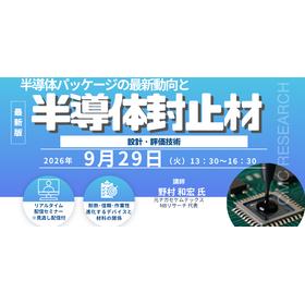
| Date and time | Tuesday, Sep 01, 2026 01:30 PM ~ 04:30 PM |
|---|---|
| Entry fee | Charge Participation fee: 44,000 yen (tax included) *Includes materials and on-demand viewing *For our newsletter subscribers (registration free) 39,600 yen (tax included) |
Inquiry about this news
Contact Us OnlineMore Details & Registration
Details & Registration
Related product
Distributors