An overview of advanced packaging technologies from 2.5D/3D chiplets to thermal management, reliability evaluation, and PFAS compliance.
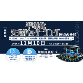
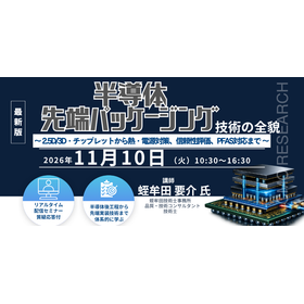
■Title: "The Full Picture of Advanced Semiconductor Packaging Technology - From 2.5D/3D and Chiplets to Thermal and Power Solutions, Reliability Evaluation, and PFAS Compliance -" ――A systematic explanation of advanced packaging technologies that support the evolution of AI semiconductors. In addition to the latest technological trends in 2.5D/3D packaging, chiplets, CoWoS, TSV, and glass core substrates, you will learn extensively about manufacturing processes, yield improvement, failure analysis, reliability evaluation, PFAS regulatory compliance, and thermal and power design. Practical case studies of failures and evaluation analysis techniques will also be detailed. - Basics and evolution of semiconductor packaging technology - Latest trends in 2.5D/3D and chiplet technology - Reliability testing and failure analysis techniques - Key points for yield improvement - PFAS regulatory compliance and sustainable materials - Thermal and power design technologies for advanced packages for AI - Engineers and researchers from the chemical, electronics, electrical, and automotive industries - Personnel involved in semiconductor backend processes and assembly technologies - Personnel involved in materials and equipment development - Those who want to systematically learn about advanced packaging technologies
Inquire About This Product
basic information
■Event Details Date and Time: November 10, 2026 (Tuesday) 10:30 AM - 4:30 PM Participation Fee: 55,000 yen (tax included) *Includes materials *Newsletter subscribers: 49,500 yen (tax included) Instructor: Yosuke Hirumuta (Hirumuta Engineering Office, Quality and Technology Consultant, Professional Engineer) Method of Attendance: This seminar will be a live-streamed seminar using "Zoom." The seminar will systematically explain the basics of semiconductor packaging, 2.5D/3D integration, chiplets, reliability evaluation, non-destructive testing, compliance with PFAS regulations, and thermal management technology for AI data centers.
Price information
Participation Fee: 55,000 yen (tax included) *Includes materials *For our newsletter subscribers (registration is free) 49,500 yen (tax included) ★If two or more people apply at the same time and all applicants register as newsletter subscribers, the participation fee per person will be half of the newsletter subscriber price.
Delivery Time
Applications/Examples of results
- 2.5D/3D package development - Evaluation and development of chiplet implementation technology - Quality improvement in semiconductor backend processes - Failure analysis and reliability assessment - Investigation of high-density implementation technology for AI - Optimization of thermal management and power supply design - Research and consideration of PFAS-compliant materials - Research and development related to semiconductor packaging and technical education *For program details and application methods, please check the related link URL.
News about this product(1)
Company information

We provide the latest industrial insights to our clients. By conducting market trend analysis, publishing technology‑related books and research reports, and organizing and managing seminars, we support research and development across a wide range of industries, with a primary focus on manufacturing. Our coverage spans diverse fields such as energy, batteries, chemicals, and biotechnology.


![[Semiconductor/Class 100 Compatible] 100% Water-Free Air Nozzle](https://image.mono.ipros.com/public/product/image/2116982/IPROS15202438644694791694.png?w=280&h=280)