
List of Semiconductor Manufacturing Equipment products
- classification:Semiconductor Manufacturing Equipment
46~90 item / All 5250 items


It won't break even after 1 million repetitions! A mat switch with reliable operation, high durability, and low price. Suitable for options in machine tools as well. Please consult us about delivery t...
- Sensors


We can accommodate high resistance over 10,000 ohms, with diameters ranging from approximately 30 mm to 8 inches, and we also offer thinning and chip processing arrangements!
- Other semiconductors
- Processing Contract
- Wafer
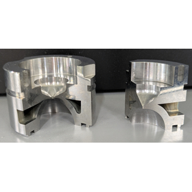

We expand possibilities with microfabrication and diffusion bonding.
- Special Processing Machinery
- Oxidation/Diffusion Device
- Heat exchanger


Visualize surface foreign substances, dirt, and scratches! It is well-received as a daily management tool for yield management, quality control, cleaning management, and hygiene management. *Demo unit...
- Visual Inspection Equipment
- Semiconductor inspection/test equipment
- Defect Inspection Equipment
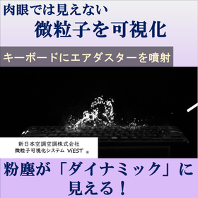
17th High-Performance Materials WEEK [Tokyo] We will be exhibiting a fine particle visualization system at the 17th High-Performance Film Exhibition. (September 30, 2026 (Wed) - October 2, 2026 (Fri) / Makuhari Messe, Hall 2)
The particle visualization technology developed under our brand "ViEST" has a very high level of detection sensitivity that allows for real-time visualization of the suspended and adhered states of micro and nano-sized particles. We are expanding our sales of visualization systems and providing evaluation services (such as investigating particles and airflow in production processes, manufacturing equipment, and factory environments, evaluating the performance of cleaning products, and proposing yield improvement measures) both domestically and internationally. We consistently support the identification of causes and the formulation of countermeasures by visualizing fine foreign substances, particle adhesion due to static electricity, and variations in cleanliness that are problematic in the film manufacturing process. The following are some examples of applications, but by utilizing our technology, we can strongly promote the resolution of various issues such as the deterioration of defect rates caused by fine foreign substances, visualization of clean airflow, and concerns regarding site cleanliness. - Visualization of foreign matter contamination and adhesion mechanisms in the coating and drying processes - Visualization of dust generation and re-adhesion during roll transportation and consideration of countermeasures - Evaluation of airflow and cleanliness within clean booths/clean rooms - Identification of dust sources within manufacturing equipment and promotion of cleanliness - Reduction of foreign matter adhesion risk on film surfaces and improvement of yield
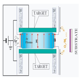

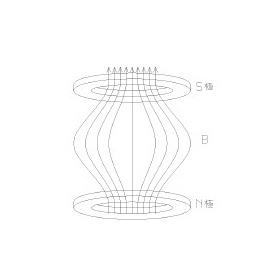
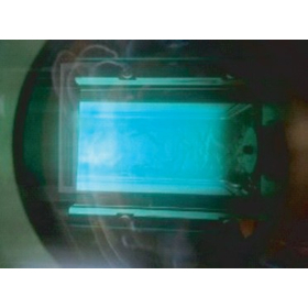
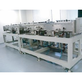
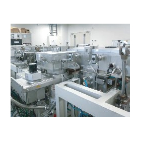
No damage to the substrate! A vacuum deposition device capable of ultra-low temperature sputtering.
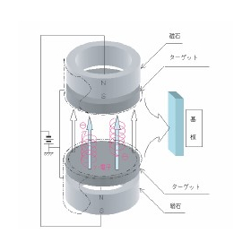
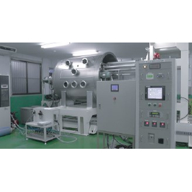
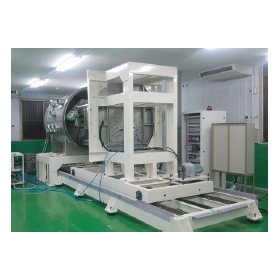
- Sputtering Equipment


Four types of products are lined up: CB type, VD type, CSH type, and SP type!
- Wafer processing/polishing equipment
- Other surface treatment equipment
- Other painting machines


We are a manufacturer specializing in filter housings.
- Other semiconductor manufacturing equipment
- Other filters
- Filtration Equipment

It is a manufacturer specializing in filter housings.
- Other semiconductor manufacturing equipment
- Other filters
- Filtration Equipment

We are a manufacturer specializing in filter housings.
- Other semiconductor manufacturing equipment
- Other filters
- Filtration Equipment


Ideal for the automation of high-precision polishing processes, deburring, chamfering, and mirror finishing! Supports specification selection according to work size and production volume!
- Wafer processing/polishing equipment
- Other surface treatment equipment

We will be exhibiting at JIMTOF2026.
Dear Sir/Madam, I would like to express my congratulations on the continued prosperity of your esteemed company. I sincerely appreciate your exceptional support. We will be exhibiting at JIMTOF2026. Focusing on the aerospace and power generation sectors, we will showcase the latest technologies, including high-precision processing of difficult-to-machine materials for aircraft engine components and power generation equipment, as well as production efficiency technologies for EVs and next-generation mobility. We kindly invite you to visit our exhibition booth and view our displays.
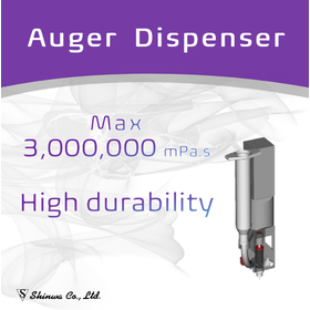

Achieving ultra-precise dispensing through screw rotation! Extensive track record and versatility in LED/line coating/3D coating!
- Bonding Equipment

Notice of Participation in Internepcon 2018: Solder Jet Demonstration! Free Samples for the First Visitors
Dear Sir/Madam, I would like to congratulate you on the continued prosperity of your company. I sincerely appreciate your exceptional support. Our company will be exhibiting at the 47th InterNEPCON Japan, which will be held at Tokyo Big Sight from January 17 (Wednesday) to January 19 (Friday), 2015. We would like to cordially invite you to see our ultra-precision dispenser equipment and high-precision dispenser (cream solder jet). All of our employees and staff are looking forward to your visit. ◎ Exhibition Booth: E7-38 <Exhibition Details> - Cream solder jet dispenser demonstration (Sample application gifts available on a first-come, first-served basis) - Proposals and displays of optimal equipment for smartphone component mounting and automotive semiconductor applications - Business negotiation room available <Contact Information> Shinwa Co., Ltd. Mechatronics System Center Contact: Ozawa TEL: 052-739-0175 E-Mail: kenji-ozawa@shinwa-jpn.co.jp
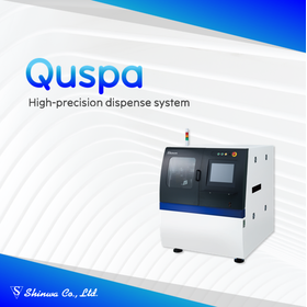
We propose a custom-made dispenser that fulfills your ideals.
- Other semiconductor manufacturing equipment
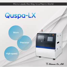
Significantly reduce tact time with continuous dispensing! The ultra-precision dispenser device 'Quspa-LX' enables high-precision fine dispensing.
- Other semiconductor manufacturing equipment

Notice of Exhibited Products and Events for Nepcon Japan 2024
We are pleased to announce that Shinwa will be exhibiting at the Internepcon Japan, which will be held from January 24 to January 26. Date: January 24 (Wed) - January 26 (Fri) 10:00 AM - 5:00 PM Location: Tokyo Big Sight, East Hall 1 Booth Number: [E4-8B] At our booth, we will be showcasing the newly redesigned dispenser device "Quspa-LX" for the first time. You will be able to see a demonstration. Additionally, we will introduce the TXC Corporation's crystal oscillators, which hold the number one global market share, and the CMOS camera modules for automotive applications from the Foxconn Group. On January 25 (Thu), the famous YouTuber Monozukuri Taro will be appearing at our booth! He will clearly explain the appeal of our new products. There will be two sessions on that day, so don't miss this opportunity! Morning: 11:00 AM Afternoon: 3:00 PM We look forward to seeing you there. Please note that pre-registration is required for entry to Internepcon Japan this year. If you have not registered, please do so via the link.
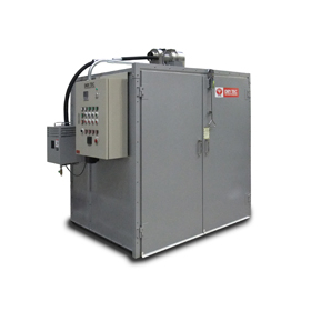

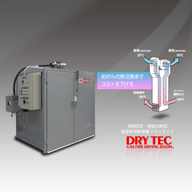
Heat recovery type, low running cost, paint drying oven.

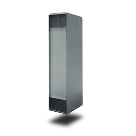
- Other painting machines
- Drying Equipment
- Annealing furnace

Dryer Dry Tech Price Information Public Site Now Available
We have launched a price information website for the painting-specific dryer, Drytech. The site features product information and sizes focused on standard models of Drytech, both front and single-door types, as well as custom products and options, including performance and price information. We have disclosed price information to facilitate a quicker process from consideration and decision-making to implementation. Please make use of it.
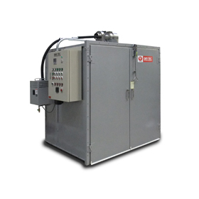
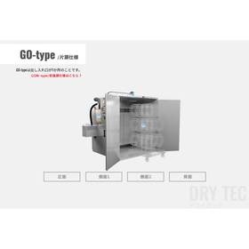
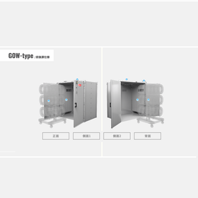
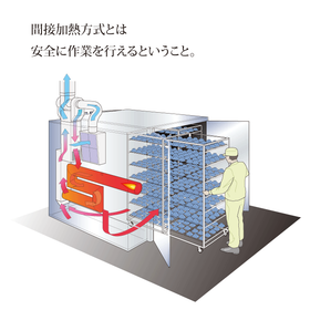
Heat recovery type, low running cost, hot air dryer for painting.
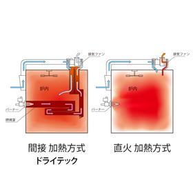
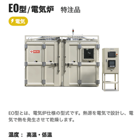
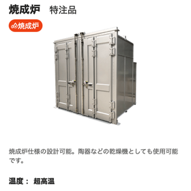
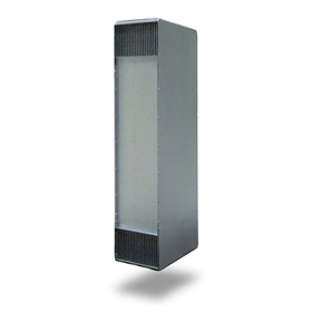
- Other painting machines
- Drying Equipment
- Annealing furnace


CVD, PVD (evaporation, sputtering, etc.) high vacuum, ultra-high temperature plate heater for wafer and small chip heating with excellent uniformity and reproducibility.
- Other semiconductor manufacturing equipment
- Annealing furnace
- CVD Equipment

◉Mini-BENCH-prism Semi-Automatic Ultra-High Temperature Experimental Furnace Max 2000℃
◉ Maximum operating temperature Max 2000℃ ◉ PLC semi-automatic control A higher model of the tabletop Mini-BENCH with semi-automatic control Automatically controls each process of "vacuum/purge cycle," "gas replacement," and "venting" Maximum operating temperature 2000℃ Semi-automatic control ultra-high temperature experimental furnace (carbon furnace, tungsten metal furnace) Compact and space-saving experimental furnace ◉ Effective heating range (crucible dimensions) - Planar heater heating range: Φ2 inch to Φ6 inch - Cylindrical heater heating range: Φ30 to Φ80 x Depth Max 100(H) mm ◉ Up to 3 MFC systems for automatic flow control (or manual adjustment) ◉ APC automatic pressure control ◉ Ensures safety during operation Monitors abnormal cooling water, chamber temperature, and overpressure. Made of SUS, the robust water-cooled chamber can be safely used even during continuous operation at maximum temperature. ◉ Compact and space-saving Width 603 x Depth 603 x Height 1,160 mm (*Installed inside rotary pump housing) Various sample heating experiments, such as ultra-high temperature heating of small samples and new material research and development, can be easily performed with simple operations. The main unit is compact yet can be used for research and development in various fields.
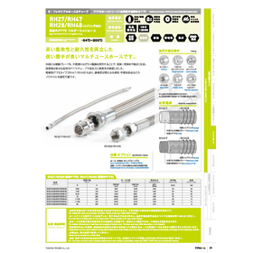

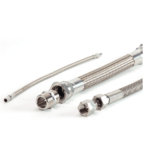
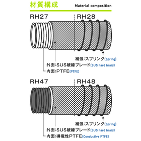
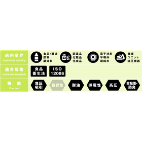
High-durability PTFE hoses achieve both high flexibility and durability through a fine wave PTFE structure. They are suitable for chemical supply lines and movable piping sections in semiconductor man...
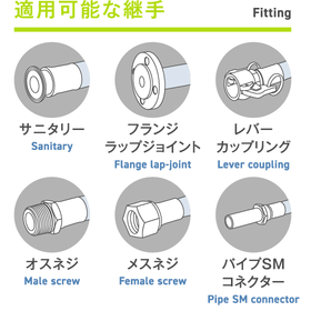
- hose
- Other semiconductor manufacturing equipment
- Etching Equipment

We are a manufacturer specializing in filter housings.
- Other semiconductor manufacturing equipment
- Other filters
- Filtration Equipment

We are a manufacturer specializing in filter housings.
- Other semiconductor manufacturing equipment

It is a manufacturer specializing in filter housings.
- Other semiconductor manufacturing equipment
- Beverage Production Equipment
- Filtration Equipment


Atomization of liquid without pressurization by piezo vibration. Enables uniform application while reducing power consumption and liquid waste.


- spray
- Coating Machine
- CMP Equipment
Start of distribution of 3D CAD data for Sonia Corporation's ultrasonic spray nozzle.
We have started distributing 3D CAD data for the Sonia ultrasonic spray nozzles. Designers and equipment manufacturers can efficiently proceed with equipment design and layout considerations by confirming product shapes and mounting dimensions in advance. This time, we have also released the 3D CAD data for the ultrasonic spray nozzles "WS40K" and "WS130K," which can be used for interference checks and design simulations before implementation. Sonia's ultrasonic spray nozzles cater to a wide range of applications, including precision coating, surface treatment, humidification, and cleaning. By providing 3D CAD data, we support the reduction of design man-hours and the shortening of development periods, facilitating a smooth process from product selection to equipment development.
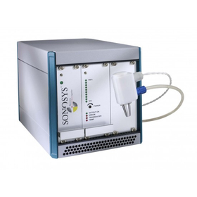
Thorough removal of fine contaminants from wafers. High-quality cleaning achieved by Sonosys.
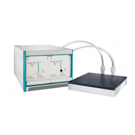
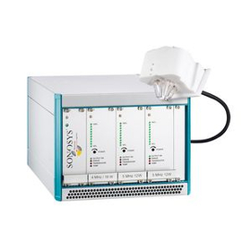
- Ultrasonic Cleaner
- Ultrasonic Oscillator
- Photomask
Announcement of the product page launch for the SONOSYS Megasonic Cleaning Nozzle System | Precision Cleaning for Semiconductors and MEMS
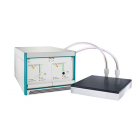
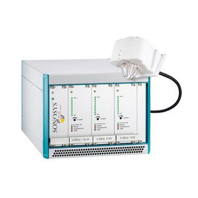
We are pleased to announce that Tick Corporation has launched a product introduction page for the SONOSYS megasonic cleaning nozzle system. The megasonic cleaning technology from SONOSYS utilizes high-frequency energy ranging from 600 kHz to 9 MHz to precisely remove fine particles while minimizing damage to microstructures such as semiconductor wafers, photomasks, and MEMS. The new page features the characteristics of single, double, and triple nozzles, as well as applications for semiconductors, MEMS, optical components, and LCD/FPD substrates. If you are considering fine particle removal, precision cleaning using ultra-pure water (DI Water), or megasonic cleaning at frequencies such as 600 kHz or 1 MHz, please take a look.
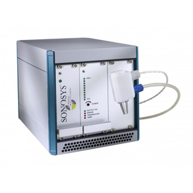
For precise cleaning of prisms. Sonosys ultrasonic cleaning device.
- Ultrasonic Cleaner
- Ultrasonic Oscillator
- Photomask
Announcement of the product page launch for the SONOSYS Megasonic Cleaning Nozzle System | Precision Cleaning for Semiconductors and MEMS
We are pleased to announce that Tick Corporation has launched a product introduction page for the SONOSYS megasonic cleaning nozzle system. The megasonic cleaning technology from SONOSYS utilizes high-frequency energy ranging from 600 kHz to 9 MHz to precisely remove fine particles while minimizing damage to microstructures such as semiconductor wafers, photomasks, and MEMS. The new page features the characteristics of single, double, and triple nozzles, as well as applications for semiconductors, MEMS, optical components, and LCD/FPD substrates. If you are considering fine particle removal, precision cleaning using ultra-pure water (DI Water), or megasonic cleaning at frequencies such as 600 kHz or 1 MHz, please take a look.
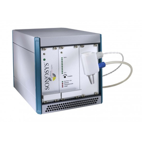
Leave the latest ultrasonic cleaning to Sonosys.


- Photomask
- CMP Equipment
- CVD Equipment
Announcement of the product page launch for the SONOSYS Megasonic Cleaning Nozzle System | Precision Cleaning for Semiconductors and MEMS
We are pleased to announce that Tick Corporation has launched a product introduction page for the SONOSYS megasonic cleaning nozzle system. The megasonic cleaning technology from SONOSYS utilizes high-frequency energy ranging from 600 kHz to 9 MHz to precisely remove fine particles while minimizing damage to microstructures such as semiconductor wafers, photomasks, and MEMS. The new page features the characteristics of single, double, and triple nozzles, as well as applications for semiconductors, MEMS, optical components, and LCD/FPD substrates. If you are considering fine particle removal, precision cleaning using ultra-pure water (DI Water), or megasonic cleaning at frequencies such as 600 kHz or 1 MHz, please take a look.

Flow spray of 2 mmlit/min or less is possible!
- nozzle
- valve
- Etching Equipment
Start of distribution of 3D CAD data for Sonia Corporation's ultrasonic spray nozzle.
We have started distributing 3D CAD data for the Sonia ultrasonic spray nozzles. Designers and equipment manufacturers can efficiently proceed with equipment design and layout considerations by confirming product shapes and mounting dimensions in advance. This time, we have also released the 3D CAD data for the ultrasonic spray nozzles "WS40K" and "WS130K," which can be used for interference checks and design simulations before implementation. Sonia's ultrasonic spray nozzles cater to a wide range of applications, including precision coating, surface treatment, humidification, and cleaning. By providing 3D CAD data, we support the reduction of design man-hours and the shortening of development periods, facilitating a smooth process from product selection to equipment development.

Next-generation megasonic technology can instantly clear wafers up to 300mm.
- Photomask
- Other semiconductor manufacturing equipment
- Ultrasonic Cleaner
Announcement of the product page launch for the SONOSYS Megasonic Cleaning Nozzle System | Precision Cleaning for Semiconductors and MEMS
We are pleased to announce that Tick Corporation has launched a product introduction page for the SONOSYS megasonic cleaning nozzle system. The megasonic cleaning technology from SONOSYS utilizes high-frequency energy ranging from 600 kHz to 9 MHz to precisely remove fine particles while minimizing damage to microstructures such as semiconductor wafers, photomasks, and MEMS. The new page features the characteristics of single, double, and triple nozzles, as well as applications for semiconductors, MEMS, optical components, and LCD/FPD substrates. If you are considering fine particle removal, precision cleaning using ultra-pure water (DI Water), or megasonic cleaning at frequencies such as 600 kHz or 1 MHz, please take a look.
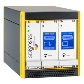
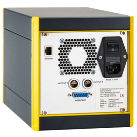
The Digital Generator is a digital control generator compatible with megasonic cleaning systems for semiconductors, electronic components, and precision instruments.
- Photomask
- Other semiconductor manufacturing equipment
- Wafer
Announcement of the product page launch for the SONOSYS Megasonic Cleaning Nozzle System | Precision Cleaning for Semiconductors and MEMS
We are pleased to announce that Tick Corporation has launched a product introduction page for the SONOSYS megasonic cleaning nozzle system. The megasonic cleaning technology from SONOSYS utilizes high-frequency energy ranging from 600 kHz to 9 MHz to precisely remove fine particles while minimizing damage to microstructures such as semiconductor wafers, photomasks, and MEMS. The new page features the characteristics of single, double, and triple nozzles, as well as applications for semiconductors, MEMS, optical components, and LCD/FPD substrates. If you are considering fine particle removal, precision cleaning using ultra-pure water (DI Water), or megasonic cleaning at frequencies such as 600 kHz or 1 MHz, please take a look.