8/5 Webinar: Semiconductor Packaging Technology Course
 CMC RESEARCH Ltd.
■Title
"Changes in Joint Structures and Packaging Responses Due to the Evolution of Semiconductors ~ Response of Resin Sealing Technology to the Increase in the Number of Joints and Narrow Pitching ~"
In semiconductor packages, which are advancing in high integration, high density, and three-dimensionality, addressing the increase in joints (bumps) and narrowing of pitches has become an important challenge. In this seminar, experienced instructors will organize the changes in joint structures accompanying the evolution of semiconductor packages and explain the latest trends, challenges, and countermeasures in resin sealing technology and mounting technology.
【Knowledge Gained from the Seminar】
- Development history and latest trends of semiconductor packaging
- Changes in joint structures and packaging technology
- Evaluation methods for resin sealing materials and sealing technology
- Sealing technology for narrow pitch bumps and reliability improvement
- Challenges and countermeasures in advanced packaging
【Target Audience】
Engineers, researchers, and sales representatives from semiconductor-related companies, as well as those involved in semiconductor manufacturing, mounting, sealing materials, and packaging technology.
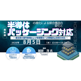
| Date and time | Wednesday, Aug 05, 2026 |
|---|---|
| Entry fee | Charge Tuition fee: 44,000 yen (tax included) *Includes materials *For our newsletter members (registration is free) 39,600 yen (tax included) ★【Newsletter Member Benefit】 If two or more people apply at the same time and all applicants are newsletter members (registration is free), the participation fee per person will be half of the newsletter member price. |
Inquiry about this news
Contact Us OnlineMore Details & Registration
Details & Registration
Related product
Distributors